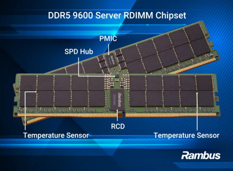
Rambus Inc. (NASDAQ: RMBS) unveiled on July 8, 2026 its DDR5 9600 Server Registered Dual Inline Memory Module chipset, built around the new sixth-generation Registering Clock Driver known as RCD06 that delivers a 20 percent increase in data rate over the prior generation and enables RDIMMs to operate at up to 9600 megatransfers per second. The complete chipset architecture includes the RCD06 alongside the PMIC5030 power management integrated circuit, a Serial Presence Detect Hub with integrated temperature sensor, and dedicated Temperature Sensor ICs, delivering a fully integrated memory interface solution designed specifically for the emerging class of agentic AI, large language model inference, and high-performance computing workloads that are structurally reshaping server memory requirements. The San Jose, California-based chip and silicon intellectual property provider positioned the release explicitly against the memory bandwidth constraints that are becoming the primary bottleneck in AI data center architectures, particularly as key-value caching techniques for LLM inference push memory capacity and bandwidth demands substantially higher than conventional server workloads support.
Rambus Inc. shares closed at 109.64 dollars on July 8, 2026, giving the company a market capitalisation of approximately 12 billion dollars against fully diluted share count near 110 million, and the announcement lands roughly 19 days before the scheduled Q2 fiscal 2026 earnings release on July 27, 2026, at which management will report on the second-quarter product revenue and licensing billings guidance previously communicated at 95 to 101 million dollars and 76 to 82 million dollars respectively. For a company that has been progressively positioning itself as the memory interface pure-play beneficiary of AI-driven server capex, the DDR5 9600 chipset launch is the operational proof point that the technology roadmap remains ahead of the mainstream AI infrastructure demand curve.
What does the Rambus DDR5 9600 Server RDIMM chipset actually change for AI data center memory bandwidth
The DDR5 9600 Server RDIMM chipset represents a substantive step function increase in server memory bandwidth capability rather than an incremental refresh of existing product lines. The 9600 megatransfers per second data rate is 20 percent higher than the prior generation solution and moves the top-tier server memory speed into a range that has previously been available only through specialty custom designs or through the fastest client memory modules. Server memory has historically lagged client memory speeds because of the additional design complexity, signal integrity requirements, and reliability specifications that server platforms demand. Rambus Inc. is delivering a chipset that closes that gap and gives server manufacturers a validated production-ready solution rather than a bespoke engineering exercise.
The mechanistic explanation for why AI workloads need this specific bandwidth increase sits in the architecture of large language model inference. LLM inference requires substantial memory bandwidth to move model weights, activations, and intermediate representations between DRAM and CPU cache hierarchies, and modern inference optimisation techniques such as key-value caching further amplify these requirements by storing and repeatedly accessing contextual data across sequential token generation cycles. Every new generation of frontier language models scales these demands, and the specific bottleneck shifts from raw compute capacity toward the ability of the memory subsystem to feed data to the compute layer fast enough to keep it utilised. That is precisely the constraint the RDIMM 9600 chipset is designed to relax.
The strategic implication for Rambus Inc. is that the company is positioning itself squarely in the segment of AI infrastructure spending where memory bandwidth economics are becoming the primary system-level design consideration. Amazon Web Services, Microsoft Azure, Google Cloud, Meta Platforms, and specialised AI infrastructure operators are increasingly making server procurement decisions based on memory bandwidth per dollar and memory bandwidth per watt rather than on CPU compute alone, and Rambus Inc.’s complete chipset solution addresses that decision framework directly. The AI-specific positioning also differentiates Rambus Inc.’s memory interface business from adjacent semiconductor peers whose products serve broader server market segments with less specific AI infrastructure alignment.
Why is the 20 percent bandwidth increase in the RCD06 the analytically important number in this release
The 20 percent bandwidth increase delivered by the RCD06 sixth-generation Registering Clock Driver is the single number that anchors the commercial and analytical case for the chipset launch. In memory interface economics, incremental bandwidth improvements typically translate directly into pricing power because they compress the number of DIMMs required to serve a given aggregate memory bandwidth requirement in a server. A 20 percent bandwidth improvement means server manufacturers can either build the same aggregate bandwidth with fewer memory slots or build higher aggregate bandwidth in the same physical envelope, both of which support the commercial case for premium pricing on the chipset itself.
The technical differentiation embedded in the RCD06 architecture reflects Rambus Inc.’s long-standing focus on signal integrity, timing precision, and clock distribution at ever-higher data rates. Scaling DDR5 memory beyond 6400 megatransfers per second introduces increasingly severe technical challenges including signal degradation, clock jitter, timing instability, and thermal management complexity. Solving those challenges at 9600 megatransfers per second is fundamentally a mixed-signal design problem that requires deep expertise in high-speed serial interfaces, and Rambus Inc. has been building that expertise over multiple generations of DDR product cycles. The RCD06 is the culmination of that engineering roadmap for the current DDR5 generation.
The commercial positioning against competing memory interface providers matters for how the announcement should be interpreted. Rambus Inc. competes in the RDIMM interface chip market against Montage Technology and Renesas Electronics Corporation, both of which produce competing register clock driver and power management chipset offerings. Delivering a validated 9600 megatransfers per second complete chipset ahead of competing offerings supports Rambus Inc.’s ability to win design-in decisions at server original equipment manufacturers including Dell Technologies Inc., Hewlett Packard Enterprise Company, Lenovo Group Limited, and Super Micro Computer, Inc. Those design-in wins convert into multi-year product revenue streams that sustain the company’s growth trajectory.
How does the complete chipset architecture with PMIC5030 and SPD Hub simplify RDIMM design economics
The complete chipset approach that Rambus Inc. has adopted is analytically differentiated from a component-only strategy. The chipset combines the RCD06 with the PMIC5030 power management integrated circuit, an SPD Hub with integrated temperature sensor, and dedicated temperature sensor integrated circuits, delivering an integrated solution that addresses the full memory module design challenge rather than requiring memory module manufacturers to source and validate multiple components from different suppliers. That integration reduces bill of materials cost, simplifies qualification testing, and improves system reliability through coherent thermal and power management design.
The PMIC5030 component addresses a specific design challenge that becomes increasingly acute as memory speeds scale. At 9600 megatransfers per second, DDR5 memory modules require efficient high-current power delivery at low voltage levels, and any inefficiency in the power management architecture translates directly into thermal stress, timing variability, and reliability degradation. The dedicated PMIC5030 design solves that challenge as an integrated part of the chipset rather than requiring memory module manufacturers to design around a general-purpose power management component. That integration is worth premium pricing to memory module makers because it reduces both design cost and time to market for their own products.
The SPD Hub and temperature sensor components address the module telemetry and thermal monitoring requirements that server platform reliability now demands. Server platforms increasingly require detailed real-time monitoring of memory subsystem health, and the integrated SPD Hub with temperature sensing provides the data pipeline that server management systems need to maintain platform reliability under sustained AI inference workloads. Continuously operating AI inference workloads impose different thermal profiles than conventional server workloads, and monitoring capability that scales with the increased thermal density is a specific competitive advantage of the complete chipset architecture.
What role does KV caching in large language model inference play in the RDIMM 9600 addressable market
Key-value caching is one of the most important optimisation techniques used to accelerate large language model inference at scale, and its widespread deployment across production LLM serving infrastructure has become one of the primary drivers of the incremental memory bandwidth demand that Rambus Inc.’s DDR5 9600 chipset is designed to serve. In LLM inference, each generated token depends on the full context of previously generated tokens, and computing the attention mechanism against that context is one of the most computationally expensive parts of the inference process. Key-value caching stores the intermediate representations of previously computed context in memory so that they can be reused across subsequent token generation without recomputation.
The memory bandwidth implications of key-value caching are substantial. As LLM context windows have scaled from a few thousand tokens to hundreds of thousands or millions of tokens, the memory footprint of the key-value cache has grown proportionally, and the bandwidth required to move key-value cache data between DRAM and the compute layer during each inference step has become one of the primary determinants of overall inference throughput and latency. Every 20 percent improvement in server memory bandwidth translates directly into either faster inference latency at fixed cost or lower cost per token at fixed latency, both of which are directly monetisable improvements for the LLM inference operators.
The addressable market implication is that the DDR5 9600 RDIMM chipset serves a segment of the server market that is growing substantially faster than the overall server market. AI inference deployments at hyperscale cloud providers, at specialised AI infrastructure operators like CoreWeave Inc. and DigitalOcean Holdings, Inc., and at enterprise customers deploying private AI infrastructure are all growing at rates that materially exceed the traditional enterprise server market growth rate. Rambus Inc.’s alignment with this specific growth segment provides a durable revenue expansion driver that supports the current valuation multiple even as broader semiconductor cyclicality creates volatility in adjacent product categories.
Why is the Rambus memory interface franchise structurally different from the NAND and DRAM manufacturer story
Rambus Inc. operates a fundamentally different business model from the NAND flash and DRAM manufacturers that dominate broader memory sector attention. SanDisk Corporation, Micron Technology, Inc., SK Hynix Inc., Samsung Electronics Co., Ltd., and Kioxia Holdings Corporation manufacture memory chips at scale and earn revenue that scales with memory pricing cycles and manufacturing capacity. Rambus Inc. does not manufacture memory chips. It designs the interface chips that sit on memory modules and enable those memory chips to communicate with server processors at high speeds. The economics are structurally different, and the exposure to memory cyclicality is meaningfully lower.
The revenue architecture that follows from this positioning delivers more stable margins and less volatile earnings than the memory manufacturer business model. Product revenue at Rambus Inc. is anchored on interface chip shipments that grow with server DIMM shipments rather than with memory bit shipments or spot memory pricing. Licensing revenue is anchored on royalty streams from intellectual property licensed to semiconductor manufacturers, and those licensing streams are typically structured with long contract durations and predictable payment schedules. The combined revenue mix is materially more predictable than the pure memory manufacturer revenue mix, and it delivers gross margins that consistently exceed the memory manufacturer averages across full memory cycle periods.
The strategic implication is that Rambus Inc. captures the value of memory demand growth without bearing the cyclical volatility of memory pricing. In the current AI-driven memory supercycle, both memory manufacturers and memory interface providers are benefiting from strong demand growth. However, when the supply and demand balance eventually normalises, the memory interface franchise should experience less pricing pressure and less earnings volatility than the memory manufacturer franchises because interface chip volumes are more anchored to server unit shipments than to memory pricing dynamics. That structural advantage supports a more premium valuation multiple than the memory sector average, and it is one of the reasons Rambus Inc. equity has been progressively re-rating through the current AI infrastructure cycle.
How does the Q1 2026 performance and $786 million cash position support the July 27 earnings setup
Rambus Inc. reported first-quarter 2026 GAAP revenue of 180.2 million dollars, with product revenue of 88.0 million dollars up 15 percent year over year and licensing billings of 70.8 million dollars, generating 83.2 million dollars of cash from operations and GAAP diluted earnings per share of 0.55 dollars. The company ended the first quarter with 786.1 million dollars of cash, cash equivalents, and marketable securities, representing a substantial balance sheet position that gives management significant capital allocation flexibility across strategic investment, share repurchase, and continued research and development scaling. The financial position supports a strong operational setup entering the second quarter earnings release on July 27, 2026.
The second-quarter fiscal 2026 guidance previously communicated is anchored on product revenue of 95 to 101 million dollars and licensing billings of 76 to 82 million dollars against a fully diluted share count of 110 million. The DDR5 9600 Server RDIMM chipset launch and the earlier May 2026 DDR5 9600 Client Chipset launch are unlikely to contribute meaningful revenue in the second quarter itself since design-in cycles and initial production ramp typically extend across multiple quarters. The commercial contribution from these product introductions will begin to materialise in the third fiscal quarter and beyond, which is the strategic argument for holding the equity through the earnings release.
The earnings release commentary that will matter most includes forward guidance on product revenue trajectory into the second half of fiscal 2026 and into fiscal 2027, updates on customer design-in wins across the new DDR5 9600 chipset portfolio, commentary on licensing billing growth from PCIe 7.0 Switch IP and other intellectual property products, and any capital allocation signalling around the 786.1 million dollar cash position. Each of these variables will shape sell-side estimate revisions following the earnings release, and the combined revision impact is likely to be positive if the current AI-driven memory bandwidth demand thesis continues to build.
What are the competitive and execution risks that could complicate the RDIMM 9600 commercial ramp
The primary competitive risk sits with Montage Technology, which operates from a strong position in the Chinese market and has been expanding its international presence through DDR5 chipset offerings that compete directly with Rambus Inc.’s product portfolio. Montage Technology has been particularly aggressive on pricing in select customer segments, and any material design-in win by Montage Technology at a major server original equipment manufacturer could compress the addressable market share available to Rambus Inc. through the current chipset generation. Renesas Electronics Corporation also competes in the segment, though with a less concentrated focus on memory interface chips relative to Montage Technology and Rambus Inc.
The execution risk on the commercial ramp includes both manufacturing capacity for the RCD06, PMIC5030, and SPD Hub components and customer qualification timing for the complete chipset. Server memory modules require lengthy qualification cycles at server original equipment manufacturers before design-in wins convert into production revenue, and any friction in that qualification process, whether related to sample availability, engineering support responsiveness, or specification revisions, can delay the revenue trajectory that supports the current valuation. Rambus Inc. has been investing in customer engineering support infrastructure to manage this qualification cycle, but the mid-2026 launch timing means the majority of design-in wins will show up in fiscal 2027 revenue rather than in the current fiscal year.
The broader market risk is that the AI infrastructure capital expenditure cycle could moderate more quickly than the current consensus assumes, either because of slower AI application revenue conversion, hyperscaler capital discipline, or macroeconomic conditions that pressure enterprise IT budgets. Rambus Inc.’s memory interface franchise is closely tied to server DIMM shipment volumes, and any material slowdown in server unit shipments would compress product revenue growth even if the memory interface content per server continues to expand. Managing that exposure through geographic and end-market diversification is one of the operational priorities that the company has been signalling in recent investor communications.
Key takeaways on what the Rambus chipset launch signals for memory interface investors and AI capex
- Rambus Inc. announced on July 8, 2026 its DDR5 9600 Server Registered Dual Inline Memory Module chipset built around the new sixth-generation Registering Clock Driver known as RCD06, delivering a 20 percent bandwidth increase over the prior generation and enabling RDIMMs to operate at up to 9600 megatransfers per second.
- The complete chipset architecture combines the RCD06 with the PMIC5030 power management integrated circuit, a Serial Presence Detect Hub with integrated temperature sensor, and dedicated Temperature Sensor ICs, delivering an integrated solution that addresses the full memory module design challenge for advanced AI data center servers.
- The chipset is specifically positioned against the memory bandwidth constraints that key-value caching in large language model inference is imposing on server memory subsystems, targeting the fastest-growing segment of server capital expenditure aligned with agentic AI and high-performance computing workloads.
- Rambus Inc. shares closed at 109.64 dollars on July 8, 2026, giving the company a market capitalisation of approximately 12 billion dollars against fully diluted share count near 110 million, and the launch precedes the Q2 fiscal 2026 earnings release scheduled for July 27, 2026.
- The Q1 2026 results delivered GAAP revenue of 180.2 million dollars, product revenue of 88.0 million dollars up 15 percent year over year, cash from operations of 83.2 million dollars, GAAP diluted earnings per share of 0.55 dollars, and a balance sheet position of 786.1 million dollars in cash, cash equivalents, and marketable securities.
- The Q2 fiscal 2026 guidance previously communicated is anchored on product revenue of 95 to 101 million dollars and licensing billings of 76 to 82 million dollars, with the DDR5 9600 chipset commercial contribution expected to materialise in fiscal 2027 as design-in cycles complete and production ramps.
- The Rambus Inc. memory interface franchise operates a fundamentally different business model from the NAND flash and DRAM manufacturer businesses of SanDisk Corporation, Micron Technology, Inc., SK Hynix Inc., Samsung Electronics Co., Ltd., and Kioxia Holdings Corporation, delivering more stable margins and less exposure to memory pricing cyclicality.
- Competitive dynamics against Montage Technology and Renesas Electronics Corporation in the memory interface chip segment will shape the addressable market share available to Rambus Inc. through the current DDR5 chipset generation, with customer design-in wins at Dell Technologies Inc., Hewlett Packard Enterprise Company, Lenovo Group Limited, and Super Micro Computer, Inc. serving as the primary competitive signalling data points.
- Execution risks include the multi-quarter server memory module qualification cycle at server original equipment manufacturers, the manufacturing capacity coordination across the RCD06, PMIC5030, and SPD Hub component supply chain, and the pace at which AI infrastructure capital expenditure translates into server DIMM shipment volumes.
- The DDR5 9600 chipset launch reinforces the strategic thesis that Rambus Inc. is positioned as a memory interface pure-play beneficiary of AI-driven server capital expenditure, with the chipset generational cadence, licensing revenue durability, and balance sheet flexibility supporting the case for continued equity re-rating as the AI inference workload thesis continues to build.
Discover more from Business-News-Today.com
Subscribe to get the latest posts sent to your email.