



Artificial intelligence has trained investors to measure semiconductor progress in ever-smaller process nodes, but much of the physical world still depends on chips manufactured using technologies that are several generations removed from the leading edge. Cars, industrial equipment, power systems, communications hardware and data-centre infrastructure require large quantities of analog, power-management and mixed-signal semiconductors whose value depends less on transistor density than reliability, voltage handling and cost.
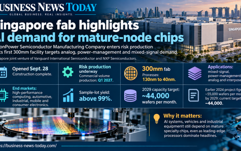
VisionPower Semiconductor Manufacturing Company Pte. Ltd. (VSMC), the Singapore joint venture between Vanguard International Semiconductor Corporation and NXP Semiconductors N.V. (NASDAQ: NXPI), opened its first 300mm fabrication facility on September 28. Construction is complete and the plant has entered risk production, with commercial volume production scheduled to begin in the first quarter of 2027.
The most interesting detail is what the factory will manufacture. Its planned processes span 130 nanometres to 40 nanometres and are intended for mixed-signal, power-management, analog and interposer applications serving markets including high-performance computing, automotive, industrial, mobile and consumer electronics.
The project therefore exposes a second semiconductor investment cycle running beside the race for advanced AI processors. Leading-edge computing may receive most of the headlines, but the electrical systems surrounding those processors and the machines into which AI increasingly moves still need enormous quantities of comparatively mature specialty silicon.
Why manufacture mature-node chips on modern 300mm wafers?
Process node and wafer diameter describe different aspects of semiconductor manufacturing. A 40nm chip does not have to be produced on an older 200mm wafer simply because its transistor technology is mature, and manufacturers can move suitable products onto 300mm wafers when the economics justify doing so.
Larger wafers allow more die to be processed in a manufacturing cycle, potentially reducing unit costs when production volumes are high enough to keep expensive equipment efficiently utilised. SEMI has noted that the cost advantages of 300mm manufacturing can apply to high-volume devices including power-management integrated circuits and other products with sufficient die size and demand.
The economic trade-off is important because 300mm factories require substantial capital. Mature-node products with modest volumes may remain better suited to fully depreciated 200mm facilities, while high-volume specialty devices can justify newer 300mm capacity if wafer utilisation and yields are strong enough.
VisionPower Semiconductor Manufacturing Company’s first sample lot achieved yields above 99%, according to the joint venture’s opening announcement. That is an encouraging manufacturing milestone, although sample-lot yield should not be treated as proof that sustained high-volume production will immediately achieve the same economics when the fab begins its commercial ramp.

Why do artificial-intelligence systems still need large quantities of mature chips?
A high-end accelerator performs the calculations inside an AI server, but it cannot regulate its own power supplies, control every sensor, interface with every physical system or manage the hundreds of lower-level electronic functions surrounding a computing platform.
Power-management integrated circuits convert and regulate electricity. Analog devices translate real-world signals into forms digital processors can use, while mixed-signal chips combine analog and digital functions in applications ranging from vehicles to factory equipment and communications systems.
That means growth in advanced computing can indirectly create demand for semiconductor categories manufactured on older nodes. The same relationship becomes more visible in physical AI, where robots, autonomous machines and intelligent industrial systems combine powerful processors with motors, sensors, power electronics and control circuitry.
NXP Semiconductors explicitly links the Singapore fab to intelligent-edge and physical-AI applications while also emphasising automotive and industrial demand. The opportunity is therefore not that mature-node chips suddenly replace leading-edge processors, but that every sophisticated system requires a wider semiconductor ecosystem than its most expensive compute device.
Why is NXP Semiconductors using a joint venture instead of building the fab alone?
When the project was announced in 2024, Vanguard International Semiconductor Corporation planned to hold 60% of the joint venture and NXP Semiconductors the remaining 40%. The initial buildout was then anticipated to cost approximately $7.8 billion, with Vanguard International Semiconductor Corporation contributing $2.4 billion of equity and NXP Semiconductors $1.6 billion, alongside additional partner contributions and third-party financing.
The structure allows NXP Semiconductors to secure capacity without funding and operating the entire fabrication complex itself. Vanguard International Semiconductor Corporation brings specialty-foundry manufacturing expertise, while underlying process technologies were planned to be licensed and transferred from Taiwan Semiconductor Manufacturing Company.
That fits NXP Semiconductors’ hybrid manufacturing strategy, which combines internal and affiliated capacity with external foundries rather than attempting to manufacture every chip itself. At the September opening, NXP Semiconductors said the project improves geographic resilience, supply control and cost competitiveness.
The resilience argument has become more significant since pandemic-era semiconductor shortages exposed how concentrated specialty-chip capacity could disrupt automobile and industrial production. Owning contractual access to geographically diversified manufacturing can therefore have strategic value even when the chips themselves use mature technologies.
Why did the current 2029 capacity target change from the figure announced in 2024?
The original 2024 announcement projected output of approximately 55,000 300mm wafers per month by 2029. The September 2026 opening announcement now states that full capacity is expected to reach approximately 44,000 wafers per month by 2029, while NXP Semiconductors said its own planned manufacturing capacity at the joint venture remains unchanged.
The difference matters because older project figures remain widely repeated after development plans evolve. The current 44,000-wafer target should therefore be treated as the controlling figure for the fab unless the joint venture publishes another revision.
The opening announcement does not provide a detailed reconciliation explaining the difference from the original gross-output target. It would consequently be speculative to attribute the change to one particular customer, process mix or engineering decision without further disclosure.
What is clear is that the facility is further advanced than a construction-stage proposal. It has completed construction, processed sample wafers and entered risk production, meaning the next test shifts from building the factory toward qualifying products, ramping volume and maintaining yields.
Is the shift to 300mm mature-node production happening beyond this one Singapore fab?
VisionPower Semiconductor Manufacturing Company is part of a broader expansion of 300mm manufacturing. SEMI’s latest outlook says worldwide 300mm front-end fab-equipment spending is projected to reach a record $149 billion in 2026, with artificial intelligence, high-performance computing, automotive demand and supply-chain diversification among the investment drivers.
Not all of that spending is directed toward mature analog and power devices because leading-edge logic and memory remain major components of 300mm investment. However, SEMI has documented a growing use of 300mm wafers for power and other specialty semiconductor categories where sufficiently high volumes can make the larger-wafer economics attractive.
This creates an important distinction in semiconductor strategy. Mature process technology does not necessarily mean mature manufacturing economics, because factories can still be redesigned around automation, larger wafers, geographic diversification and lower unit cost.
The opportunity therefore sits between two misleading extremes. Mature-node devices are neither obsolete leftovers from an earlier semiconductor era nor automatic beneficiaries of every AI investment cycle; they are essential supporting components whose manufacturing base is being modernised where demand and economics justify the transition.
What does NXP Semiconductors’ recent share performance suggest?
NXP Semiconductors shares closed at $243.66 on October 2, up 1.87% for the day and approximately 3.1% above the $236.32 close on September 28, when the VisionPower Semiconductor Manufacturing Company opening was announced. The stock nevertheless remained well below its May 2026 high, showing that the recent recovery has occurred within a more mixed year for semiconductor investors.
It would be inappropriate to attribute the several-day gain specifically to the Singapore fab because NXP Semiconductors is exposed to global automotive, industrial and electronics demand as well as wider semiconductor-market movements. The plant will also require time to move from risk production into meaningful commercial output.
Investors can instead monitor a clearer set of operational milestones: volume production beginning in the first quarter of 2027, product qualification, utilisation rates, yield stability and the progression toward approximately 44,000 wafers per month by 2029.
The semiconductor industry’s most visible battle may continue to be fought at the smallest process nodes, but the physical systems powered by artificial intelligence will need far more than GPUs. VisionPower Semiconductor Manufacturing Company shows why another layer of semiconductor investment is occurring several generations behind the leading edge, where larger wafers and mature process technology can still produce strategically important innovation.
Discover more from Business-News-Today.com
Subscribe to get the latest posts sent to your email.