


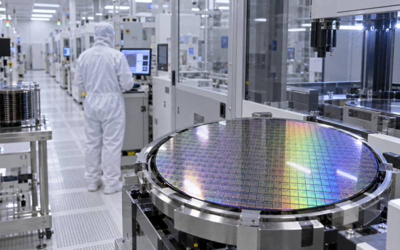
Applied Materials, Inc. (NASDAQ: AMAT) has unveiled its Equipment and Process Innovation and Commercialization Center in Sunnyvale, California, advancing a semiconductor research initiative with planned capital investment expected to reach approximately $5 billion as customer projects commence. The October 12, 2026, opening brings major chip manufacturers, equipment suppliers and university researchers together inside a 600,000-square-foot facility dedicated to accelerating next-generation manufacturing technologies. The initiative positions Applied Materials to play a more integrated role in developing semiconductor processes for artificial intelligence, advanced memory and high-performance computing. Its commercial significance will depend on whether collaborative research shortens development cycles and generates additional demand for Applied Materials equipment and services.
The EPIC Center represents a substantial change in how Applied Materials intends to collaborate with its largest customers, particularly as semiconductor manufacturing becomes more complex and expensive. Instead of developing equipment in relative isolation before customers test it in production environments, the company wants engineers from across the semiconductor supply chain to work on emerging technologies together.
The reported $5 billion commitment is not a newly announced cash expenditure completed on opening day. Applied Materials has clarified that capital spending is expected to scale toward that amount over time as projects involving customers move forward.
Why is Applied Materials bringing the world’s largest chipmakers into one research facility?
The EPIC Center has been designed to address an increasingly expensive problem facing the semiconductor industry: translating laboratory innovations into reliable, commercially manufacturable technologies. Advanced processors require complicated combinations of materials, structures, interconnections and packaging systems, often involving research teams working across different organisations. Transferring technologies between development environments can create delays, particularly when equipment and materials interact differently at increasingly small dimensions.
Applied Materials is attempting to reduce those handoffs by placing materials scientists, equipment engineers, semiconductor manufacturers and researchers within a common development infrastructure. The facility incorporates nearly four acres of cleanroom space, giving participants access to environments relevant to advanced semiconductor manufacturing. This approach could allow customers to identify process limitations earlier, refine equipment designs and improve the transition from experimental processes to production-ready solutions.
The founding chipmaker partners include Taiwan Semiconductor Manufacturing Company, Intel Corporation, SK hynix, Micron Technology and Samsung Electronics. Other participating organisations include Broadcom, Advantest, SCREEN Holdings, KIOXIA and BE Semiconductor Industries, alongside research institutions such as Stanford University, the University of California, Berkeley, and the University of California, Los Angeles.
These partnerships connect companies working on different parts of the semiconductor technology stack, from logic and memory to testing and advanced packaging. Their participation does not necessarily establish guaranteed purchase commitments for future equipment, but it provides Applied Materials with opportunities to align its research priorities with actual customer requirements.
For equipment suppliers, becoming involved earlier in product development can be commercially valuable because manufacturing technology decisions often influence spending across successive generations of semiconductor production. Successful collaboration could increase the probability that Applied Materials processes become part of customers’ future manufacturing roadmaps, although individual equipment purchases will still depend on technical performance and commercial economics.
How could the EPIC Center accelerate AI processors, advanced memory and semiconductor packaging?
Artificial intelligence hardware increasingly depends on improvements beyond conventional transistor scaling. Faster processing requires advanced packaging, high-bandwidth memory, sophisticated electrical interconnections and technologies capable of limiting energy consumption. These requirements create opportunities for materials engineering companies because performance improvements often depend on multiple manufacturing steps being optimised together.
Taiwan Semiconductor Manufacturing Company intends to use its collaboration with Applied Materials to advance technologies relevant to future manufacturing nodes, interconnections and packaging. Intel Corporation has similarly identified increasingly complex semiconductor architectures as a reason to strengthen collaboration between manufacturing and equipment specialists. Both companies stand to benefit from research arrangements that reduce repeated development work, provided shared projects deliver measurable production improvements.
Memory manufacturers face a related but distinct challenge. Artificial intelligence accelerators require high-bandwidth memory and increasingly sophisticated memory integration, while conventional dynamic random-access memory and NAND storage also continue evolving. Collaboration involving Micron Technology, SK hynix, Samsung Electronics and KIOXIA gives Applied Materials visibility into several major technology transitions rather than tying the facility’s prospects to a single chip category.
Advanced packaging provides another potential growth opportunity. As semiconductor manufacturers combine different computing components within increasingly integrated systems, bonding, materials deposition, interconnection and precision manufacturing become more consequential. Applied Materials’ collaboration with BE Semiconductor Industries on hybrid bonding illustrates how its research strategy extends beyond traditional front-end wafer processing.
The wider commercial opportunity is not simply faster chips. A manufacturing process that improves yield, reduces defects or enables more efficient integration may lower the effective cost of computing even if the initial equipment becomes more sophisticated. For semiconductor manufacturers committing billions of dollars to new production capacity, relatively modest improvements in production yield can create meaningful financial benefits.
What do Applied Materials’ latest financial results reveal about its capacity to fund semiconductor innovation?
Applied Materials enters the EPIC Center’s opening phase with substantial existing semiconductor equipment revenue and profitability. For its third fiscal quarter ended July 26, 2026, the company reported record revenue of approximately $9.12 billion, representing 25% growth from the corresponding period a year earlier. GAAP operating income reached approximately $3.08 billion, with an operating margin of 33.7%, compared with 30.6% a year earlier.
The company’s Semiconductor Systems segment generated approximately $7.04 billion in quarterly revenue, up from $5.56 billion in the comparable prior-year period. Its Applied Global Services segment contributed approximately $1.78 billion, indicating that the business derives revenue from both new manufacturing equipment and services supporting installed systems. That combination provides commercial exposure to semiconductor investment cycles as well as recurring customer requirements.
Applied Materials also reported approximately $2.33 billion in non-GAAP free cash flow during the quarter. Although a single quarter’s cash generation should not be treated as a permanent funding rate, the figure illustrates the scale of operating resources available to support research programmes alongside other corporate commitments.
A $5 billion research initiative is substantial even for a company with Applied Materials’ earnings capacity. The economics will depend on the pace of capital deployment, the cost of operating sophisticated development infrastructure and the eventual commercial value of the technologies produced. Management has indicated that spending will increase as customer projects commence, meaning the financial commitment should be assessed over multiple periods rather than compared with one quarter’s earnings alone.
Research expenditure does not automatically translate into near-term revenue. Customer qualification, factory investment decisions and process integration can take considerable time, especially for advanced semiconductor nodes. EPIC’s potential value therefore lies partly in helping Applied Materials influence future equipment requirements before those requirements turn into purchase orders.
Why could the research model strengthen Applied Materials’ competitive position in AI chip manufacturing?
The semiconductor equipment industry includes companies with highly specialised capabilities in lithography, deposition, etching, inspection and other manufacturing processes. Customers often rely on combinations of technologies from different suppliers, creating complex integration requirements. Applied Materials’ ambition is to become more deeply involved in resolving those requirements at the research stage rather than competing solely when manufacturers procure individual systems.
This model could strengthen customer relationships by making Applied Materials a collaborative development partner across multiple generations of technology. Engineers participating in shared projects may gain a clearer understanding of the company’s equipment capabilities, while Applied Materials obtains insight into future manufacturing challenges. Such relationships could improve research efficiency and inform product investment decisions, although commercial contracts and intellectual property arrangements will remain important.
The presence of competing chip manufacturers inside the same wider research ecosystem also introduces practical considerations. Companies must protect confidential manufacturing information while still benefiting from collaborative work on materials and equipment. Applied Materials will need to demonstrate that its partnership structure can support commercially sensitive development without undermining customers’ intellectual property protections.
Competition will not disappear because manufacturers participate in a common research environment. Rival equipment suppliers can continue developing alternative manufacturing technologies, and customers may retain multiple vendors to improve supply-chain resilience and pricing flexibility. The competitive advantage would become more defensible if EPIC-generated technologies achieve measurable performance improvements and subsequently enter high-volume semiconductor production.
The EPIC Center could also deepen the American semiconductor research ecosystem by connecting industrial companies with universities and equipment development infrastructure. However, expanding domestic research capabilities does not mean that the resulting chips will necessarily be manufactured in the United States. Commercial production locations will continue to depend on customers’ factory networks, economics, government incentives and manufacturing requirements.
Why did Applied Materials shares remain under pressure despite the $5 billion announcement?
Applied Materials shares closed at approximately $497.53 on October 12, declining 1.87% during the session even as the company unveiled its new research facility. The decline occurred during a period of weakness across parts of the semiconductor sector, making it difficult to isolate any single announcement as the cause of the movement. The stock’s reaction suggests that investors were weighing broader market and technology-sector conditions rather than automatically assigning incremental near-term value to the facility opening.
The disconnect between operational expansion and daily share performance is understandable because the EPIC investment is a long-duration strategic initiative. The company already has substantial exposure to semiconductor equipment spending, and its recent quarterly results show strong revenue and margin growth. Near-term valuation remains sensitive to customer capital expenditure, memory demand, advanced manufacturing investment and the profitability of existing operations.
The October unveiling also follows previously announced collaborations and development work associated with the EPIC programme. Consequently, the opening represents an operational milestone rather than the first disclosure of the underlying investment strategy. Investors evaluating Applied Materials will need to separate the symbolic importance of the facility from changes in future earnings expectations.
The most meaningful indicators of commercial success will emerge from the technologies developed through the research partnerships. Evidence that EPIC is shortening qualification cycles, improving manufacturing yields or contributing to substantial customer equipment orders would make the programme’s financial contribution easier to assess.
Applied Materials has established a major collaborative research platform at a time when artificial intelligence is raising the technological demands placed on semiconductor manufacturers. Its latest financial results provide a strong operating foundation, but the facility’s strategic value will become clearer only as participating customers move new technologies from joint development into commercial manufacturing. The first persuasive evidence will be a demonstrable production improvement or equipment adoption tied to research conducted through EPIC.
What are the key takeaways from the Applied Materials $5 billion EPIC Center opening?
- Applied Materials unveiled the EPIC Center on October 12, 2026.
- Planned capital investment is expected to reach approximately $5 billion over time.
- The 600,000-square-foot facility includes nearly four acres of cleanroom space.
- Founding partners include major logic and memory chip manufacturers.
- The research model aims to reduce delays between innovation and manufacturing.
- Advanced packaging, memory and AI computing are major technology priorities.
- Third-quarter fiscal 2026 revenue reached approximately $9.12 billion.
- Commercial returns will depend on successful technology qualification and customer equipment adoption.
- The next measurable test is whether EPIC research translates into manufacturing improvements and equipment demand.
Discover more from Business-News-Today.com
Subscribe to get the latest posts sent to your email.