


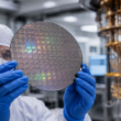


GlobalFoundries Inc. (NASDAQ: GFS) has qualified its SLATE wafer-to-wafer bonding technology on the company’s 9SW radio-frequency silicon-on-insulator platform, bringing advanced 3D integration closer to volume production for next-generation RF front-end modules. The technology is manufactured at GlobalFoundries’ 300mm facility in Singapore and is expected to ramp to volume production in the second half of 2027. The announcement matters because RF chipmakers are under pressure to deliver smaller, more power-efficient components for 5G mobile devices, satellite connectivity and other wireless applications where board space, battery life and signal performance are increasingly strategic. GFS recently traded around $83.27, within an intraday range of $82.42 to $86.29, giving GlobalFoundries a market value of about $45.9 billion as investors assess whether differentiated specialty semiconductor platforms can support steadier growth beyond commodity chip cycles.
Why does GlobalFoundries’ SLATE qualification matter for RF semiconductor growth?
GlobalFoundries’ SLATE qualification matters because radio-frequency semiconductors are becoming more complex as 5G, satellite communications, connected devices and physical AI applications expand. Mobile and wireless devices need front-end modules that handle multiple frequency bands, reduce power consumption and fit into increasingly compact form factors. That creates a technical and commercial opportunity for foundries that can help customers integrate more RF functionality into smaller chip footprints.
SLATE is designed to address that challenge through wafer-to-wafer bonding. By allowing two 9SW wafers to be bonded and vertically integrated, GlobalFoundries can help designers stack large field-effect transistors in a more compact architecture. The company says the technology can reduce overall die size by up to 45%, which is commercially relevant because board space is one of the most valuable constraints inside smartphones, wearables, connected devices and satellite-capable mobile hardware.
The platform also strengthens GlobalFoundries’ positioning in specialty semiconductors. Unlike leading-edge logic foundries that compete heavily on node shrinks, GlobalFoundries has built its market identity around differentiated technologies such as RF-SOI, FD-SOI, silicon germanium, embedded non-volatile memory, power management and specialty process platforms. SLATE gives the company another way to deepen that moat by combining process technology with advanced packaging.
For investors, the significance is not that one technology qualification will immediately transform revenue. The more important point is that GlobalFoundries is trying to capture value where customers need performance, power efficiency, design enablement and manufacturing reliability. That can support a more defensible business model than competing only on wafer volume.
How could 9SW SLATE improve next-generation 5G front-end module design?
9SW SLATE could improve next-generation 5G front-end module design by enabling more compact integration of RF components used in switches, low-noise amplifiers and antenna tuners. These components are essential in mobile devices because they help manage wireless signals across multiple bands and use cases. As devices support more frequencies and more complex connectivity features, front-end modules can become crowded and difficult to scale through conventional design methods.
The 9SW RF-SOI platform is GlobalFoundries’ most advanced RF solution for front-end modules, covering sub-8GHz and FR3 frequency ranges for 5G mobile devices and satellite communications. That matters because future wireless devices will need to operate across more demanding spectrum environments while preserving battery life and thermal efficiency. A technology that can reduce design area while supporting RF performance gives customers a practical tool for product differentiation.
The efficiency angle is also important. GlobalFoundries says 9SW delivers more than 20% improvement in efficiency through lower on-resistance and off-capacitance, while also reducing standby currents. Those metrics matter for device makers because power loss in RF components can affect battery performance, heat and user experience. Better RF efficiency becomes more valuable as devices handle more data and stay connected across more network modes.
The qualification also gives chip designers a clearer path to prototype and plan around 9SW SLATE. An integrated process design kit is available through the GF Connect portal, and 9SW and 9SW SLATE are available for prototyping through the GlobalShuttle multi-project wafer program. That design enablement is important because technology adoption depends not only on process readiness, but on whether customers can begin designing products with confidence.
Why does advanced packaging matter for GlobalFoundries’ specialty foundry strategy?
Advanced packaging matters for GlobalFoundries because semiconductor performance is increasingly shaped by integration rather than transistor scaling alone. Customers want smaller devices, better efficiency, stronger connectivity and lower system-level cost. For specialty applications such as RF, power, photonics, automotive and IoT, the value often comes from combining mature or differentiated technologies in smarter ways. SLATE fits directly into that strategy.
The industry has already seen advanced packaging become central in AI accelerators and high-performance computing. GlobalFoundries’ move shows that packaging innovation is also becoming important in RF and wireless systems. Wafer-to-wafer bonding can help overcome scaling and integration limits where conventional two-dimensional layouts become inefficient. That broadens the role of packaging from back-end assembly into a design-enabling technology.
For GlobalFoundries, the advantage is that advanced packaging can deepen customer relationships. A foundry that provides process technology, design enablement and integration capability becomes harder to replace than a foundry that only supplies standard wafer capacity. This can be especially valuable in long-lifecycle markets where customers prioritize reliability, supply security and platform continuity.
SLATE also creates a roadmap beyond 9SW. GlobalFoundries says the technology can support future heterogeneous 3D integration across differentiated technologies including FD-SOI, RF-SOI and silicon germanium. That could eventually open opportunities in data centers, satellite connectivity, IoT and mobile devices. Investors should not assume every roadmap item becomes commercial revenue, but the direction strengthens the company’s specialty platform narrative.
How does the Singapore manufacturing base support GlobalFoundries’ RF roadmap?
GlobalFoundries’ Singapore manufacturing base supports the RF roadmap because 9SW SLATE is being manufactured at the company’s 300mm facility in Singapore. That matters because RF-SOI customers need manufacturing consistency, scale and long-term supply availability. Specialty semiconductor platforms often serve high-volume device markets, and customers need confidence that a technology can move from prototyping to production without major supply-chain disruption.
Singapore is an important part of GlobalFoundries’ global manufacturing footprint. The company operates across the United States, Europe and Asia, giving customers geographic diversity at a time when semiconductor supply-chain resilience remains a boardroom issue. For RF customers serving global mobile, satellite and IoT markets, manufacturing location and capacity planning can influence sourcing decisions.
The expected volume production ramp in the second half of 2027 gives customers a planning horizon. Device and RF front-end module design cycles require early engagement, design kits, prototyping and qualification before commercial deployment. By announcing production readiness now, GlobalFoundries is giving customers time to evaluate 9SW SLATE for future wireless products.
The Singapore base also ties into the broader semiconductor supply-chain debate. Governments and customers are increasingly looking for manufacturing partners with global scale, regional diversification and trusted production capability. GlobalFoundries’ ability to manufacture specialty technologies across multiple regions can support its positioning in markets where supply security matters as much as raw performance.
What does GFS stock performance suggest about investor expectations for GlobalFoundries?
GFS stock performance suggests investors are valuing GlobalFoundries as a differentiated foundry with AI, automotive, connectivity and specialty semiconductor exposure, but not as a pure leading-edge logic growth stock. The shares recently traded around $83.27, with intraday movement between $82.42 and $86.29. The company’s market value of about $45.9 billion reflects a sizable semiconductor platform, but one where investors still watch margin performance, utilization, customer demand and specialty technology adoption closely.
The SLATE announcement supports the higher-quality part of the GFS story. Investors want to see GlobalFoundries compete in areas where it can earn durable returns through differentiated processes and customer partnerships. RF-SOI is one of those areas because device makers need proven specialty platforms for connectivity, mobile and satellite applications. A stronger RF roadmap can support confidence in future design wins.
The stock will not trade on SLATE alone. Investors will still focus on revenue growth, wafer demand, capacity utilization, gross margin, capital spending and customer concentration. Specialty foundries are not immune to semiconductor cycles, and weakness in consumer electronics or industrial demand can affect results. However, technologies such as 9SW SLATE can help GlobalFoundries make the case that its business is tied to structural growth areas rather than only near-term chip demand.
The broader market has become more selective in semiconductor investing. Companies with direct AI accelerator exposure have received the most attention, but the AI and connectivity economy also needs power-efficient RF, sensors, embedded systems, data movement and edge connectivity. GlobalFoundries is trying to position itself as an enabler of that wider physical AI infrastructure. The challenge is proving that narrative through sustained customer adoption and financial performance.
Which commercial hurdles could shape 9SW SLATE adoption?
The main commercial hurdle for 9SW SLATE is customer design adoption. Even when a technology is production-ready, chip designers need time to evaluate performance, cost, yield, reliability and integration benefits. RF front-end modules are performance-sensitive, and customers will not adopt a new platform unless it improves product economics or solves a real design constraint. GlobalFoundries must show that the smaller die size and integration benefits translate into meaningful advantages for customers.
Cost will also matter. Advanced packaging and wafer-to-wafer bonding can add complexity, and customers will compare total cost against the benefits of reduced die size, board space and improved performance. If SLATE helps customers shrink module size or improve efficiency enough to support better end-device performance, the cost case becomes stronger. If the benefits are too incremental, adoption may be slower.
Competition is another factor. RF semiconductor markets include major suppliers and foundry partners with strong technical capabilities. GlobalFoundries must convince customers that 9SW SLATE offers a better combination of performance, efficiency, manufacturability and design enablement. Cadence’s design enablement support through Virtuoso Studio can help customers evaluate the technology, but competitive differentiation will still depend on product-level outcomes.
Timing could also shape adoption. Volume production is expected in the second half of 2027, which means the technology is aimed at future product cycles rather than immediate revenue acceleration. Investors should view the announcement as a medium-term platform milestone. The value will become clearer as customers prototype, qualify and potentially design 9SW SLATE into next-generation wireless products.
What does the SLATE milestone signal for the broader semiconductor industry?
The SLATE milestone signals that semiconductor innovation is spreading across process technology, packaging, design enablement and system-level integration. The industry is no longer defined only by who can produce the smallest transistor node. In many high-growth markets, value is created by integrating the right technologies efficiently and reliably. RF front-end modules, automotive chips, IoT devices, satellite communications and edge AI systems all depend on that kind of specialty innovation.
This trend can benefit foundries with differentiated platforms. GlobalFoundries is not trying to outspend the largest leading-edge logic players at the most advanced nodes. It is trying to build defensible positions in markets where customers need power efficiency, RF performance, longevity, reliability and secure supply. SLATE strengthens that approach by adding a 3D integration tool to an already established RF-SOI platform.
The announcement also reflects the growing importance of compact, power-efficient wireless hardware. As 5G evolves and satellite connectivity expands into mobile and IoT devices, RF front-end modules must support more functions in less space. That creates demand for technologies that can reduce die size while preserving or improving performance. GlobalFoundries is aiming directly at that bottleneck.
For the broader sector, this is another example of how advanced packaging is moving beyond headline AI chips. Packaging innovation is becoming a cross-market enabler, touching wireless, data centres, satellite, IoT and mobile devices. GlobalFoundries’ SLATE technology shows that even mature and specialty semiconductor categories are being reshaped by 3D integration. That could make specialty foundries more strategically important in the next phase of chip industry growth.
Key takeaways on what GlobalFoundries’ 9SW SLATE milestone means for GFS and RF semiconductors
- GlobalFoundries has qualified SLATE wafer-to-wafer bonding technology on its 9SW RF-SOI platform.
- The technology supports advanced 3D integration for compact, high-performance RF front-end modules.
- 9SW SLATE is manufactured at GlobalFoundries’ 300mm facility in Singapore.
- Volume production is expected to ramp in the second half of 2027.
- SLATE can reduce overall die size by up to 45% by enabling designers to stack and integrate large field-effect transistors vertically.
- The 9SW RF-SOI platform supports sub-8GHz and FR3 frequency ranges for 5G mobile devices and satellite communications.
- The technology targets RF applications such as switches, low-noise amplifiers and antenna tuners.
- GlobalFoundries is positioning SLATE as part of a broader 3D integration roadmap across RF-SOI, FD-SOI and silicon germanium technologies.
- GFS recently traded around $83.27, giving the company a market value of about $45.9 billion.
- The main investor test is whether GlobalFoundries can turn specialty platform innovation into customer design wins, stronger margins and more durable growth.
Share this:
Discover more from Business-News-Today.com
Subscribe to get the latest posts sent to your email.