


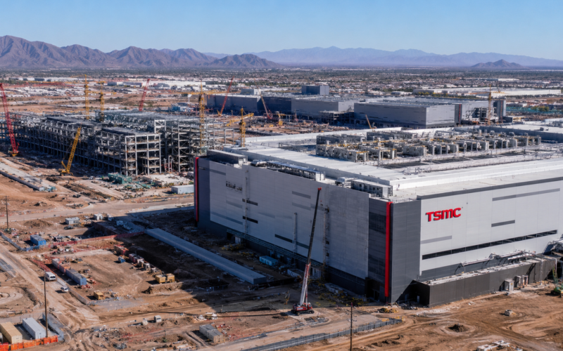
The TSMC Arizona Semiconductor Manufacturing Project has become one of the most strategically important industrial developments in the United States because it sits at the intersection of artificial intelligence, chip supply security, Taiwan-U.S. geopolitics and advanced manufacturing capacity. The project is located in Phoenix, Arizona, where Taiwan Semiconductor Manufacturing Co., through TSMC Arizona Corporation, is building a leading-edge semiconductor manufacturing cluster on a campus of more than 1,100 acres.
The project began as a much smaller U.S. manufacturing plan and then expanded into a three-fab commitment worth more than $65 billion, supported by up to $6.6 billion in CHIPS Act direct funding and up to $5 billion in available loans. That first major federal-support phase covers leading-edge logic fabs designed around N4, N3, N2 and A16 technologies, with NIST also listing N5 among the process technologies included in the award framework.
By 2026, the project had moved well beyond its initial footprint. TSMC’s first Arizona fab entered high-volume production on N4 process technology in the fourth quarter of 2024, the second fab structure was completed in 2025 with N3 volume production targeted for the second half of 2027, and the third fab, slated for N2 and A16 technologies, broke ground in April 2025 with volume production targeted by the end of the decade. TSMC also says the fourth fab and first advanced packaging fab entered the initial stages of construction in early 2026.
The biggest change came in July 2026, when TSMC announced another major Arizona expansion. Arizona Commerce Authority said the additional $100 billion plan would lift TSMC’s total Arizona investment to $265 billion and described the long-term footprint as 10 fabs, two advanced packaging facilities and an R&D center. TSMC’s own Arizona project page frames the currently underway plan as six semiconductor logic wafer fabs, two advanced packaging facilities and an R&D center, while also noting the company’s July 2026 intent to build several more logic wafer fabs for 2-nanometer and below technologies.
That makes TSMC Arizona much more than a single fab project. It is becoming a long-cycle semiconductor manufacturing platform intended to support American demand for advanced chips, especially as AI infrastructure spending increases demand for leading-edge logic and advanced packaging.
Why is TSMC Arizona becoming America’s biggest advanced chipmaking test?
TSMC Arizona is becoming America’s biggest advanced chipmaking test because it asks whether the United States can rebuild part of the world’s most complex manufacturing stack without recreating the full Taiwanese ecosystem that made TSMC dominant. The project has money, customers, policy support and strategic urgency, but its success depends on execution at a scale the U.S. semiconductor sector has not attempted in decades.
The Phoenix campus is not just another industrial development. It is a test of whether leading-edge chip production can be localised in a higher-cost market while still meeting the yield, reliability and delivery standards demanded by AI, cloud computing, smartphone and high-performance computing customers.
The project also tests the limits of industrial policy. The CHIPS Act can reduce the cost burden and accelerate domestic capacity, but it cannot by itself create experienced semiconductor construction labour, process engineers, equipment technicians, chemical supply chains, advanced packaging expertise and operational know-how.
That is why TSMC Arizona matters beyond Phoenix. If the project scales successfully, it could become the anchor of a durable U.S. advanced semiconductor ecosystem. If it struggles with cost, labour, infrastructure or yield pressure, it will show how difficult it is to rebuild leading-edge chip manufacturing outside its strongest Asian clusters.

Where is TSMC building its Phoenix semiconductor campus?
The TSMC Arizona Semiconductor Manufacturing Project is located in Phoenix, Arizona, in the north of the city. The site is part of a growing semiconductor and advanced manufacturing corridor that has become one of the most important chip industry clusters in the United States.
The campus spans more than 1,100 acres and is designed as a multi-fab semiconductor production base rather than a single factory. TSMC Arizona Corporation is the operating entity, while parent company Taiwan Semiconductor Manufacturing Co. remains the global technology and capital-allocation driver behind the project.
The location matters because Phoenix offers land, road access, power infrastructure, links to suppliers, proximity to universities and workforce programmes, and a state government that has actively positioned Arizona as a semiconductor manufacturing hub. Arizona Commerce Authority says the state has attracted more than 70 semiconductor expansions since 2020, representing more than $314 billion in investment across manufacturing, equipment, materials, packaging, R&D and workforce development.
For the United States, the Phoenix location also has national security relevance. Leading-edge chip manufacturing remains heavily concentrated in Taiwan, and the Arizona project is designed to bring at least some advanced logic manufacturing closer to major U.S. customers in artificial intelligence, high-performance computing, consumer electronics, automotive and connected devices.
The site’s strategic significance is therefore larger than its physical footprint. It is a test of whether the United States can rebuild part of the advanced semiconductor manufacturing stack at scale while still relying on TSMC’s Taiwan-centred technology development and global foundry model.
Who controls TSMC Arizona and why does ownership matter?
The project is owned and operated through TSMC Arizona Corporation, a subsidiary of Taiwan Semiconductor Manufacturing Co. TSMC is the world’s dominant pure-play foundry and manufactures chips for a large base of fabless and system-company customers.
The Arizona project is not an independent U.S. chip company. It is an overseas manufacturing expansion by TSMC, which means the core technology, process roadmap, customer relationships and capital discipline remain connected to the Taiwanese parent company.
That ownership model is central to the project’s importance. The United States wanted advanced manufacturing capacity onshore, but the most advanced foundry capability remains concentrated at TSMC. Arizona therefore gives U.S. customers domestic production access without requiring them to switch away from the foundry ecosystem that already supports many leading AI, mobile and high-performance computing chips.
TSMC’s own messaging connects the project to customers such as Apple, NVIDIA, AMD, Broadcom and Qualcomm. That customer base is important because the investment is not being built in isolation. It is tied to demand from companies that need advanced process technology for AI accelerators, data-centre chips, mobile processors, networking silicon and other high-value semiconductor products.
The project also sits within a larger U.S. policy framework. The U.S. Department of Commerce awarded TSMC Arizona up to $6.6 billion in CHIPS Act direct funding for the initial three-fab cluster, with milestone-based disbursement tied to construction, production and commercial performance.
Which chip technologies will TSMC produce in Arizona?
TSMC Arizona is being built as a leading-edge semiconductor manufacturing cluster. The initial three-fab project is designed to produce advanced logic chips using N4, N3, N2 and A16 process technologies, while later expansion plans add more logic fabs, advanced packaging facilities and an R&D centre.
The first fab is already in high-volume production on N4 process technology. N4 is used for high-performance computing, mobile and other advanced applications where power efficiency, transistor density and performance matter.
The second fab is targeted for N3 process technology, with volume production expected in the second half of 2027. N3 is a major node for AI and high-performance computing because it delivers strong power, performance and area improvements for advanced chips.
The third fab is slated for N2 and A16 technologies, with volume production targeted by the end of the decade. N2 introduces nanosheet transistor technology, while A16 combines TSMC’s N2 nanosheet process with backside power delivery features aimed at improving performance and power characteristics for high-performance computing applications.
The later expansion is important because semiconductor value increasingly depends not only on wafer fabrication, but also on advanced packaging. AI chips require dense chip-to-chip connectivity, high-bandwidth memory integration and system-level packaging. TSMC’s Arizona advanced packaging plans are therefore critical if customers want more of the AI chip supply chain to be completed inside the United States.
How far has the TSMC Arizona project advanced in 2026?
The latest status shows TSMC Arizona moving from an initial advanced manufacturing foothold into a much larger U.S. semiconductor cluster. TSMC’s current Arizona project timeline says the first fab began high-volume production on N4 in the fourth quarter of 2024, the second fab structure was completed in 2025, and N3 volume production is targeted for the second half of 2027.
The third fab has also advanced. TSMC broke ground on the third fab in April 2025, and the facility is slated for N2 and A16 technologies by the end of the decade. TSMC Arizona also celebrated the topping of its third fab in May 2026, marking a major structural milestone for the building.
The July 2026 expansion announcement changed the project’s scale again. Arizona Commerce Authority said TSMC planned to invest another $100 billion in Arizona, bringing total planned Arizona investment to $265 billion. The authority described the long-term plan as 10 fabs, two advanced packaging facilities and an R&D centre, although TSMC’s own project page describes six logic fabs, two packaging facilities and an R&D center as the current plans underway, with additional fabs intended under the July expansion.
Reuters also reported that TSMC’s first Arizona fab was operational and achieving yields as good as the company’s flagship Taiwan fab, according to TSMC Chief Financial Officer Wendell Huang. The same update said the second fab would shortly begin equipment move-in, construction was underway on the third fab, and preparatory work had started on the fourth fab and the first advanced packaging facility.
The key point for 2026 is that TSMC Arizona is no longer a promise based mainly on site work and policy ambition. One fab is already producing, the second is moving toward equipment and 2027 volume production, the third is under construction, and later-stage expansion has begun to reshape the project’s long-term role.
Why does TSMC Arizona matter for AI chip supply?
TSMC Arizona matters for artificial intelligence because advanced AI systems depend on leading-edge logic chips. Training and inference workloads require powerful processors, graphics processing units, networking chips and high-performance compute components that are usually made on advanced process nodes.
TSMC is central to this ecosystem because many of the world’s leading AI and high-performance computing companies rely on its foundry capacity. The Arizona project gives those customers a path to source at least some leading-edge chips from U.S.-based production.
The project also addresses a supply-chain concentration problem. Much of the most advanced semiconductor manufacturing remains in Taiwan, creating geopolitical and business-continuity risks for companies and governments. TSMC Arizona does not eliminate that dependence, but it reduces the all-or-nothing character of the risk by creating an American manufacturing base for selected advanced nodes.
The advanced packaging component is especially important for AI. Modern AI accelerators are not only about single chips. They often depend on complex packaging that brings together compute dies, memory, interconnects and substrates. Without advanced packaging, domestic wafer fabrication alone would not fully localise the AI chip supply chain.
That is why the later expansion beyond wafer fabs matters. If TSMC Arizona can combine leading-edge wafer production with advanced packaging capacity, the project could support a more complete U.S.-based supply route for some high-value AI chips.
How much CHIPS Act support is behind TSMC Arizona?
The CHIPS Act is supporting the initial TSMC Arizona expansion through federal incentives administered by the U.S. Department of Commerce. The Department awarded TSMC Arizona up to $6.6 billion in direct funding to support more than $65 billion of investment in three greenfield leading-edge fabs in Phoenix.
The award also includes up to $5 billion in available loans. Funding disbursement is linked to capital expenditures and to construction, production and commercial milestones, which means the incentives are structured around project execution rather than simple upfront payment.
The CHIPS support is important because advanced semiconductor fabs are among the most capital-intensive industrial assets in the world. They require massive spending on cleanroom buildings, lithography tools, process equipment, chemicals, gases, ultrapure water systems, power systems, waste treatment and highly skilled labour before meaningful output begins.
For Washington, the funding is not simply economic development. It is intended to strengthen U.S. economic and national security by bringing some leading-edge semiconductor manufacturing capacity onto American soil. The Department of Commerce has specifically linked the project to artificial intelligence, high-performance computing, consumer electronics, automotive systems and Internet of Things applications.
For TSMC, the CHIPS Act support reduces the financial burden of building in a higher-cost overseas environment. The project still depends on TSMC’s commercial discipline and customer demand, but federal incentives help close part of the cost gap between Arizona and TSMC’s more mature manufacturing base in Taiwan.
Can Phoenix build the workforce needed for a $265bn chip cluster?
The initial three-fab phase is expected to create about 6,000 direct high-tech manufacturing jobs, more than 20,000 accumulated construction jobs and tens of thousands of indirect jobs. Phoenix officials and TSMC-related updates also indicate that the Arizona operation already employs thousands of full-time workers.
The job impact extends beyond direct fab staff. Semiconductor fabs need tool installers, electricians, mechanical contractors, process engineers, facility engineers, chemical suppliers, gas suppliers, materials companies, equipment service teams, safety specialists, logistics providers and cleanroom construction expertise.
The supplier effect is already part of Arizona’s broader semiconductor positioning. The Arizona Commerce Authority says the state has attracted semiconductor expansions across leading-edge manufacturing, equipment, materials suppliers, advanced packaging, R&D and workforce development since 2020.
The workforce challenge is equally important. Reuters reported that TSMC sees constraints around construction labour and infrastructure as it expands in Arizona. That is a critical issue because fabs are built in phases, and each new building requires highly specialised construction labour and equipment installation expertise.
If the project succeeds, Phoenix could become one of the most important semiconductor workforce centres in North America. If labour, training, housing, water, power and infrastructure constraints tighten, the same scale that makes TSMC Arizona strategically powerful could also become an execution risk.
Can TSMC Arizona manage water, power and environmental pressure?
TSMC Arizona is being built in a desert state, so water use is one of the most important public-interest issues around the project. Advanced semiconductor manufacturing requires ultrapure water, recycling systems and wastewater treatment, making water management central to long-term acceptability.
TSMC says that, at startup, approximately 65% of the water used in the Arizona operation will come from in-house water recycling systems. The company also says it is building an Industrial Water Reclamation Plant at the Phoenix operation, expected to be completed in 2028, with a design goal of enabling 90% or more water recycling and near-zero liquid discharge.
Power is another major issue. Leading-edge fabs require large and reliable electricity supplies for tools, cleanrooms, cooling systems, abatement systems and facility infrastructure. TSMC says the Arizona facility is installing 14.5MW of solar energy through panels that also provide covered parking and began purchasing renewable energy credits in 2023 to cover 100% of its power use.
Those measures do not remove environmental questions. Renewable energy credits are not the same as physically powering the fab entirely with on-site renewable electricity, and water recycling targets still need to be tested at full operating scale. The project’s environmental credibility will depend on actual performance as more fabs enter production.
Air emissions, chemicals, waste handling and emergency management also matter. Semiconductor fabs use complex chemical processes, and the project must operate under federal, state and local environmental protections, including National Environmental Policy Act requirements tied to federal support.
How does TSMC Arizona reshape the U.S.-Taiwan chip relationship?
TSMC Arizona changes the U.S.-Taiwan semiconductor relationship by moving part of advanced manufacturing capacity into the United States while keeping TSMC’s technology leadership anchored in Taiwan. That creates both strategic reassurance and strategic tension.
For the United States, Arizona supports the goal of reducing dependence on a single geography for advanced chips. For Taiwan, TSMC’s overseas expansion raises questions about how much advanced capability should move abroad and how much should remain at home as part of Taiwan’s economic and security position.
TSMC executives have indicated that the most leading-edge technology still requires close coordination between R&D and operations, and that Taiwan remains central to that relationship. This means Arizona should not be read as a full relocation of TSMC’s cutting-edge ecosystem.
Instead, the project is best understood as selective geographic diversification. TSMC can serve American customers with U.S.-based production while continuing to develop and ramp many of its most advanced technologies in Taiwan before transferring selected processes overseas.
That model could strengthen both sides if managed well. The United States gains more domestic chip capacity, while TSMC deepens its relationship with major customers and the U.S. government. But the balance will remain politically sensitive because semiconductors are no longer just commercial products. They are strategic assets linked to AI, defence, data centres, autonomous systems and national security.
What could still slow the TSMC Arizona buildout?
The biggest near-term risk is execution complexity. Building one leading-edge fab is difficult. Building a multi-fab cluster with advanced packaging, R&D, supplier networks, water systems, power systems and workforce pipelines is much harder.
Workforce availability is one constraint. TSMC’s expansion requires construction labour, tool installation specialists, engineers, technicians and experienced manufacturing staff. The larger the Arizona plan becomes, the more pressure it places on training systems, housing, contractors and regional infrastructure.
Cost is another challenge. U.S. semiconductor manufacturing is generally more expensive than manufacturing in established Asian clusters. Labour costs, construction costs, supplier maturity, permitting, tool logistics and operational learning curves can all affect project economics.
Technology transfer also requires careful sequencing. Advanced process nodes need deep manufacturing discipline, close engineering feedback and customer qualification. Even when a building is complete, production ramp and yield improvement can take time.
The project also faces geopolitical and regulatory risk. U.S. export controls, China-related restrictions, Taiwan policy debates and changing U.S. industrial policy could all affect customer planning and investment priorities. TSMC Arizona sits inside a global chip supply chain that is increasingly shaped by government policy as much as by customer demand.
What is the long-term outlook for TSMC Arizona?
The future outlook for TSMC Arizona is strong but highly execution-sensitive. The project has moved from policy ambition to actual production, with the first fab already making N4 chips and later fabs advancing through construction, equipment and planning stages.
The second fab is the next major milestone because N3 volume production is targeted for the second half of 2027. If that ramp proceeds well, it will strengthen confidence that Arizona can support not just one successful fab, but a broader advanced manufacturing cluster.
The third fab will be more strategically important because it is linked to N2 and A16 technologies by the end of the decade. That will test whether Arizona can support future nanosheet and backside-power-generation manufacturing at scale.
The advanced packaging facilities may become just as important as the wafer fabs. AI chips increasingly require packaging innovation, not only transistor scaling. A U.S.-based packaging layer would make the Arizona project more valuable to American AI, cloud, hardware and defence customers.
In 2026, TSMC Arizona is becoming the central test case for whether the United States can rebuild a meaningful share of leading-edge semiconductor manufacturing. The project has money, customers, federal support and operating momentum. Its hardest test now is whether Phoenix can scale from first-fab success into a full AI-era chipmaking cluster without losing cost discipline, environmental credibility or execution speed.
Discover more from Business-News-Today.com
Subscribe to get the latest posts sent to your email.