
A semiconductor manufacturing step that could require three or four masks with conventional extreme-ultraviolet lithography may eventually be completed with a single High-NA EUV exposure. That possibility has moved from research-roadmap theory toward commercial relevance because Intel Foundry is now using ASML’s 0.55 numerical-aperture technology on selected Intel 18A layers for a subset of Intel Core Ultra Series 3 processors, code-named Panther Lake. ASML said in July 2026 that those layers had been dual-qualified on High-NA EXE and conventional NXE EUV equipment in Oregon, with products manufactured using the High-NA option shipping at yields matched to the established NXE process. The milestone makes Intel the first chipmaker publicly confirmed to use High-NA EUV in high-volume logic manufacturing, but its larger significance lies in what the technology could remove from the fab rather than simply what it can print smaller.
That distinction matters because advanced semiconductor manufacturing is increasingly constrained by process complexity as much as by optical resolution. Conventional 0.33NA EUV remains capable of printing extremely small features, but the densest future structures can require multi-patterning, in which one circuit layer is divided across several masks, exposures and supporting process steps. Imec estimates that selected future A14 and A10 critical metal layers could require three or four masks with conventional EUV but potentially only one High-NA exposure. If that advantage survives the transition from experimental wafers into reliable mass production, High-NA could reduce not only lithography complexity but also alignment steps, metrology requirements, wafer movement and the number of opportunities for defects to enter some of the most difficult layers of a chip.
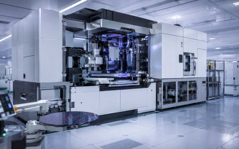
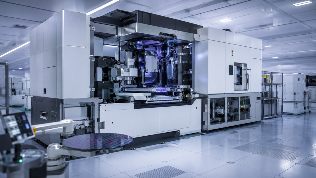
Intel’s first TWINSCAN EXE:5000 installation at its D1X research and development factory in Hillsboro, Oregon, illustrates the engineering scale required to make that possible. Intel describes the approximately 165-ton machine as roughly the size of a double-decker bus, while ASML and ZEISS SMT had to redesign major elements of the optical system to raise numerical aperture from 0.33 to 0.55 without changing the 13.5-nanometre wavelength used by today’s production EUV systems. High-NA is therefore not simply a more powerful successor to conventional EUV. It is an attempt to change the economics of how the semiconductor industry prints its hardest patterns.
What is High-NA EUV lithography and why does numerical aperture matter for advanced chips?
Semiconductor lithography transfers microscopic circuit patterns onto light-sensitive material covering a silicon wafer. ASML’s current high-volume EUV systems use 13.5-nanometre light and projection optics with a numerical aperture of 0.33, while the new EXE generation retains the same wavelength but increases numerical aperture to 0.55. In practical terms, the larger numerical aperture allows the optical system to capture a wider range of diffracted light from the mask and resolve smaller structures on the wafer.
ASML specifies an 8-nanometre resolution for the High-NA EXE platform and says the technology can print features roughly 1.7 times smaller than current NXE EUV systems. Geometrically, that corresponds to theoretical density scaling of about 2.9 times, although that figure should not be interpreted as meaning a commercial processor will automatically contain 2.9 times as many transistors in the same area. Actual chip density also depends on transistor architecture, wiring, cell design, design rules and many other process decisions.
The higher numerical aperture also increases image contrast, which matters because the ability to distinguish the intended feature from the surrounding resist becomes increasingly difficult as dimensions shrink. ASML says High-NA provides approximately 40% greater imaging contrast than its existing NXE architecture, potentially helping reduce some patterning variability while allowing difficult structures to be printed at lower exposure doses.
Achieving those gains required a new anamorphic optical design developed with ZEISS SMT. Instead of shrinking the mask pattern equally in both directions, High-NA reduces it four times along one axis and eight times along the other. That arrangement allows the industry to continue using established mask dimensions while accommodating the physically larger mirrors needed for 0.55NA optics, although it also reduces the exposure field and introduces additional considerations around stitching large patterns.
Why could High-NA EUV eliminate several masks from the hardest semiconductor layers?
The real economic argument for High-NA begins with multi-patterning. When a lithography system cannot print an increasingly dense structure in one exposure, engineers can split the original design across several masks and build the final pattern through repeated lithography and processing sequences. The approach has allowed semiconductor manufacturers to extend existing lithography systems considerably, but every additional mask can introduce another resist coat, exposure, alignment, etch, deposition or inspection step.
Imec’s latest roadmap work demonstrates why High-NA could become economically important even if the scanners themselves are more difficult and expensive to operate. For selected critical metal layers at future A14 and A10 logic generations, imec expects conventional 0.33NA EUV to require three or four masks for structures that researchers have demonstrated with a single High-NA exposure. A similar opportunity exists in future DRAM, where selected bitline-periphery and storage-node-landing-pad structures at the D1d and D0a generations could move from at least three conventional EUV masks to one High-NA exposure.
Those comparisons apply to particular critical layers rather than entire chips, but even selective process simplification can be valuable in a modern fab. Leading-edge wafers pass through hundreds of processing operations over production cycles that can stretch for months, meaning the cost of a lithography decision includes much more than scanner time alone. Eliminating masks can reduce overlay requirements, inspection stages, wafer movement and the cumulative probability that one additional process step damages yield.
The relevant commercial comparison is therefore not one High-NA scanner versus one conventional EUV scanner. It is one High-NA exposure versus the complete multi-patterning sequence a manufacturer would otherwise need to produce the same structure.
Is Intel already using High-NA EUV to manufacture commercial processors?
Yes, but only on selected layers, and that limitation is important. ASML confirmed in July 2026 that Intel Foundry had entered high-volume manufacturing using High-NA EUV on specific Intel 18A layers for a subset of Panther Lake processors. Those layers have been dual-qualified on the EXE High-NA platform and conventional NXE EUV equipment in Oregon, allowing Intel to choose between the two process routes rather than committing the entire product to the new technology.
ASML said products manufactured through the High-NA option were shipping at yields matched to the existing NXE process, which turns the milestone into something more meaningful than another lithography demonstration. Semiconductor manufacturers ultimately care less about whether a machine can print an impressive experimental feature than whether the resulting process can repeatedly produce functioning chips at acceptable yield.
Intel’s approach also offers a likely model for broader industry adoption. High-NA does not have to replace conventional EUV across an entire process node to create economic value. Chipmakers can introduce it first on a handful of layers where resolution, pattern simplification or reduced multi-patterning provides a sufficiently large advantage, while continuing to use existing NXE and deep-ultraviolet systems elsewhere.
High-NA adoption may therefore progress layer by layer rather than through wholesale replacement of an entire lithography generation.
How small have High-NA EUV systems already printed in semiconductor research?
Imec has demonstrated structures close to the nominal optical capability of the platform. In 2024, researchers using the EXE:5000 printed single-exposure 16-nanometre-pitch line-space structures in metal-oxide photoresist, corresponding to approximately 8-nanometre half-pitch, alongside contact-hole and pillar structures at 24-nanometre pitch.
The more important milestone came when researchers began converting those optical patterns into electrically functioning structures. In 2025, imec reported single-exposure High-NA patterning of 20-nanometre-pitch structures with 13-nanometre tip-to-tip dimensions, alongside ruthenium interconnects at 20- and 18-nanometre pitch. The evaluated 20-nanometre direct-metal-etch structures achieved 100% electrical test yield, while earlier work had already produced more than 90% electrical yield on selected 20-nanometre metal-line test structures.
Those results should not be confused with full-chip yield. A test structure containing a comparatively small number of patterned features is fundamentally different from a processor containing billions of transistors and many layers of interconnects. What the experiments demonstrate is that High-NA is progressing beyond impressive resist images toward electrically useful structures that resemble the dimensions future semiconductor manufacturing will require.
Why do photoresists, masks and metrology matter as much as the High-NA EUV scanner?
A scanner can create an exceptionally sharp optical image and still fail to produce an economically viable semiconductor process. The projected pattern has to interact predictably with photoresist, survive development, transfer successfully into underlying materials and be measured with enough precision to determine whether billions of repeated features remain inside extremely narrow tolerances.
This makes High-NA an ecosystem transition rather than simply an ASML equipment upgrade. Imec has identified metal-oxide resists, underlayers, hard masks, optical proximity correction, photomasks, etching, metrology and defect inspection as crucial development areas. The smaller the printed structures become, the more statistical variation in photons and resist chemistry can produce random local failures known as stochastic defects.
Exposure dose links those technical problems directly to economics. Higher doses can improve pattern formation but require the scanner to spend more time delivering EUV energy to each field, reducing throughput. Imec has demonstrated more than 20% dose reduction for selected line-space patterns by optimising resists, underlayers, masks and development conditions without increasing the evaluated roughness or stochastic failures. In separate contact-hole work, researchers reported a 6% dose reduction alongside a 30% improvement in local critical-dimension uniformity.
That means improvements in chemistry can influence the productivity of one of the semiconductor industry’s most complex pieces of capital equipment. High-NA economics will ultimately be determined by interactions across the entire process stack rather than by scanner specifications alone.
Why is imec installing its own High-NA EUV system in Belgium?
Imec received an ASML EXE:5200 High-NA system at its Leuven research facility in March 2026, where the tool is being integrated with the organisation’s NanoIC pilot line and broader 300-millimetre research infrastructure. Imec expects the scanner to be fully qualified during the fourth quarter of 2026, meaning it should still be described as an R&D and pilot-line installation rather than a high-volume production fab.
The reason the installation matters is that semiconductor manufacturers need somewhere to solve High-NA ecosystem problems without consuming scarce production capacity inside their own leading-edge fabs. Resist suppliers, mask companies, metrology vendors, etch-equipment manufacturers and chipmakers can use a common research environment to evaluate how their technologies behave around a production-relevant High-NA scanner.
That shared development model can shorten the learning cycle. Instead of every manufacturer independently discovering the same fundamental process limitations, portions of the ecosystem can be matured collectively before individual companies apply their proprietary device and process architectures.
The commercial value of imec’s EXE:5200 may therefore come less from the wafers it produces than from how much uncertainty it removes before semiconductor companies commit High-NA to expensive production nodes.
How much faster is ASML’s newer EXE:5200B High-NA lithography system?
Throughput is one of the most important areas where the second-generation system improves on the original EXE:5000. ASML’s April 2026 roadmap lists the EXE:5000 at approximately 110 wafers per hour without stitching and 75 wafers per hour with stitching at a 50 mJ/cm² exposure dose. The newer EXE:5200B increases those figures to approximately 175 wafers per hour without stitching and 135 with stitching.
The difference is commercially significant because an advanced semiconductor fab cannot afford to create a bottleneck around its most expensive patterning equipment. A machine capable of printing smaller features but exposing wafers too slowly would force manufacturers either to purchase more tools or accept lower fab output, both of which weaken the economic argument for adopting the technology.
ASML says the EXE:5200B combines higher productivity with improved overlay performance, supported by an upgraded EUV light source and projection optics developed with ZEISS SMT. Intel became the first customer to install and pass acceptance testing of an EXE:5200B, giving the company access to a platform designed much more explicitly around high-volume manufacturing than the first-generation development tool.
ASML’s roadmap already extends further, with subsequent EXE:5200C, EXE:5200D and EXE:5400E configurations targeting progressively higher productivity. That progression shows why High-NA should be viewed as a manufacturing platform still moving rapidly down its industrial learning curve rather than a fixed machine specification.
What technical problems could still slow High-NA EUV adoption?
Higher numerical aperture improves resolution but makes depth of focus tighter, reducing how much variation can be tolerated across the wafer surface and process stack. The smaller exposure field created by the anamorphic design also introduces stitching requirements when a chip pattern exceeds the available field size, while increasingly small features make random defects more consequential.
Imec continues to identify depth-of-focus optimisation, stochastic-defect mitigation, stitching, masks, resists and pattern transfer among the areas requiring further development. Each issue matters because semiconductor manufacturers need process windows that remain stable across millions of wafers, not merely isolated examples of excellent lithography.
High-NA is also competing with an incumbent technology that continues to improve. ASML is still increasing throughput and capability across its 0.33NA NXE roadmap, allowing manufacturers to extend conventional EUV through increasingly sophisticated multi-patterning where that remains more economical.
The adoption threshold is therefore continuously moving. High-NA does not have to outperform the conventional EUV process available several years ago. It has to outperform the best conventional EUV process available when a future chip actually enters production.
Will every advanced semiconductor layer eventually require High-NA EUV?
Probably not, because advanced semiconductor fabs already mix several generations of lithography according to the requirements of individual layers. Deep-ultraviolet systems remain useful for less demanding structures even in leading-edge fabs, while conventional EUV is concentrated where its resolution and process simplification justify the higher cost.
High-NA is likely to be deployed even more selectively during its early commercial years. Imec sees the strongest near-term case on future critical logic metal layers and selected DRAM structures where conventional EUV would otherwise require increasingly complex multi-patterning. Other layers can remain on NXE EUV or DUV without sacrificing product performance.
That selective model does not reduce High-NA’s strategic importance. A lithography generation can become indispensable without patterning every layer of a chip if it owns the few layers that determine whether the next process node can be manufactured economically.
The relevant question is therefore not what percentage of total wafer exposures eventually move to High-NA. It is whether the hardest and most valuable layers become difficult to manufacture competitively without it.
Could fewer masks make High-NA EUV economical despite its enormous complexity?
The optical argument is increasingly established. ASML has demonstrated the 0.55NA architecture, imec has produced electrically functioning structures at dimensions relevant to future logic and memory, and Intel has now demonstrated that selected High-NA processes can operate inside high-volume manufacturing while matching the yield of an established NXE alternative.
The remaining question is economic and must be answered at the level of the complete fab process. A semiconductor manufacturer has to compare High-NA scanner throughput, uptime and process maturity with the masks, exposures, resist processes, alignment steps, etches, inspections and additional cycle time required to create the same structure through conventional EUV multi-patterning.
For selected future structures, imec’s comparison of three or four 0.33NA EUV masks becoming one High-NA exposure shows why the equation could eventually become compelling. Removing several steps from an already extraordinarily complex manufacturing flow can create value not only through direct process cost but also through reduced overlay risk, shorter cycle time and fewer opportunities for yield loss.
That is why Intel’s 2026 production milestone matters more than another record-small experimental line. High-NA EUV spent years being described as a technology semiconductor manufacturers would eventually need once conventional EUV became too complicated to extend economically. It is now participating in the manufacture of processors that are actually shipping, while a second generation of machines is improving the throughput needed to make wider adoption practical.
The next semiconductor lithography battle is therefore no longer simply about whether High-NA can print smaller features. It is about whether one more sophisticated exposure can replace enough masks, process steps and production complexity to justify putting the world’s most advanced optical machines into the centre of tomorrow’s fabs.
Discover more from Business-News-Today.com
Subscribe to get the latest posts sent to your email.