


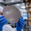


dorsaVi Limited (ASX: DVL) has commenced tape-out of its first RRAM-CMOS validation chip, moving the company’s 22-nanometre semiconductor programme from a completed design package into staged physical implementation. The chip is intended to test resistive random-access memory, write-and-verify circuits and compute-in-memory functionality using commercial CMOS front-end wafers sourced through Taiwan Semiconductor Manufacturing Company. The milestone brings dorsaVi closer to producing the physical silicon data required to assess its technology across robotics, defence systems, exoskeletons, industrial artificial intelligence and medical wearables. However, tape-out is not the same as successful silicon validation, customer adoption or commercial production. The central tension is whether dorsaVi can convert a technically ambitious semiconductor roadmap into reliable devices, commercial partnerships and revenue before development costs place additional pressure on its balance sheet.
Why does dorsaVi’s RRAM chip tape-out matter if physical silicon has not yet been validated?
Tape-out is an important semiconductor development milestone because it marks the point at which a completed integrated-circuit design is prepared for physical manufacturing. dorsaVi has moved beyond conceptual architecture and design finalisation into the process required to fabricate wafers, integrate its RRAM layer and produce chips for electrical testing.
That progress reduces one category of development risk. The company has completed a design package that can enter a commercial semiconductor implementation flow rather than remaining a simulation, laboratory concept or research proposal. It also follows the June 2026 completion of the validation chip design developed with Nanyang Technological University in Singapore and the Industrial Technology Research Institute in Taiwan.
However, the current milestone should be interpreted precisely. dorsaVi has commenced tape-out, but it has not yet reported completed fabrication, packaged devices, independent performance verification, manufacturing yield or customer qualification.
The physical silicon must still demonstrate that the RRAM memory cells, CMOS circuitry, sensing paths and compute-in-memory structures operate together under real manufacturing conditions. Semiconductor designs that appear promising in modelling can still encounter variability, reliability, yield or integration problems when converted into silicon.
For dorsaVi, the next phase is therefore more demanding than the announcement headline may initially suggest. The company is moving from design confidence into evidence generation. A successful validation chip could materially strengthen discussions with manufacturers and prospective customers. Weak or inconsistent test results could require redesign work, additional fabrication cycles and further capital.
What will the validation chip test across RRAM, CMOS and compute-in-memory functions?
Resistive random-access memory stores information through different resistance states rather than relying on the charge-storage methods used by several conventional memory technologies. Its attraction for edge artificial intelligence is that it can retain data without continuous power and potentially operate close to the point where computation occurs.
dorsaVi’s chip includes dedicated write-and-verify circuitry. After a memory cell is programmed, the circuitry is designed to check whether the cell has reached the required resistance range. A cell that remains too close to the sensing threshold can create uncertainty when the system attempts to distinguish one stored state from another.
The validation process will examine resistance-state separation, sensing margins, memory array behaviour and the effectiveness of the write-and-verify function. These tests matter because laboratory-level memory performance is not sufficient for robotics, medical or defence applications that may require consistent operation across repeated cycles and changing environmental conditions.
The chip also contains compute-in-memory structures. Conventional systems frequently move information between separate memory and processing components, creating power consumption and latency. Compute-in-memory architectures attempt to perform selected calculations within or adjacent to the memory array, reducing the need to transport data repeatedly.
dorsaVi’s design is intended to support local accumulation across as many as 64 inputs while using programmed resistance states as computing weights. The validation programme will measure circuit speed, read-access time, compute-in-memory performance and overall array-level behaviour.
These measurements will determine whether dorsaVi has produced an interesting test structure or the foundation for a scalable product platform. The distinction is commercially important. A validation chip can demonstrate basic functionality without yet meeting the durability, power, speed, accuracy and manufacturing requirements of an end customer.
How does the TSMC wafer pathway lower manufacturing barriers without proving scalability?
dorsaVi’s implementation process begins with commercial CMOS front-end wafers sourced through Taiwan Semiconductor Manufacturing Company. Semiconductor partners will then undertake the back-end-of-line process through which the RRAM layer is integrated above the underlying CMOS circuitry before wafer-level electrical testing.
This approach could reduce development barriers because it does not require dorsaVi to create an entirely new transistor manufacturing platform. The RRAM stack is designed to be incorporated into established back-end-of-line processes, potentially allowing future products to use existing foundry infrastructure.
That architecture may also provide flexibility for migration between process nodes or adaptation to different customer applications. dorsaVi has identified two potential commercial routes: embedding its technology directly into end devices or working with foundries and fabless semiconductor companies to develop specialised chips.
The reference to Taiwan Semiconductor Manufacturing Company must nevertheless be treated carefully. The current disclosure states that commercial front-end wafers are sourced through the foundry. It does not establish that Taiwan Semiconductor Manufacturing Company has endorsed dorsaVi’s intellectual property, entered a commercialisation agreement or agreed to manufacture future products at scale.
Foundry compatibility is only one element of commercial readiness. dorsaVi must also demonstrate that the added RRAM layers can be integrated consistently, that wafer yields are commercially acceptable and that performance remains stable across manufacturing variation.
The economic test is equally important. Even a technically functional device must offer enough performance or energy advantage to justify integration costs, customer redesign work and qualification timelines. A practical semiconductor platform must be manufacturable, repeatable and commercially attractive, not merely possible to fabricate.
Can dorsaVi transform from a wearable-sensor company into a semiconductor platform business?
dorsaVi’s established operations are based on wearable sensors and software used to measure human movement across clinical, occupational health and elite sports applications. Its ViMove+ platform and related products provide the company with experience in sensing, biomechanical data and devices operating close to the human body.
The semiconductor strategy represents a much broader ambition. dorsaVi is attempting to combine sensing, memory and local computation so that artificial intelligence decisions can occur on-device rather than depending continuously on cloud connectivity.
That direction creates strategic logic. Wearable devices, exoskeletons and autonomous machines require low-power processing, rapid responses and the ability to continue operating where connectivity is weak or unavailable. dorsaVi’s existing knowledge of movement sensing could help it identify specialised applications rather than compete directly in general-purpose memory.
The company has also expanded its intellectual-property position. During the March 2026 quarter, dorsaVi completed the acquisition of neuromorphic and processing-in-memory intellectual property and began discussions with commercial partners and venture capital firms in Israel. It has separately licensed human-robot collaboration technology from Nanyang Technological University, widening its intended market from human measurement into systems where people and machines operate together.
However, semiconductor development differs fundamentally from selling movement-analysis software and wearable sensors. It requires process engineering, fabrication partners, test infrastructure, intellectual-property protection, customer qualification and longer commercial timelines.
The strategic opportunity is that a successful RRAM platform could address markets much larger than dorsaVi’s historical wearable operations. The strategic risk is that management may need to support multiple technology programmes before any one of them generates meaningful licensing, product or royalty revenue.
The strongest commercial model may therefore involve partnerships rather than dorsaVi attempting to become a vertically integrated chip producer. Licensing intellectual property, co-developing application-specific devices or supplying semiconductor blocks to established manufacturers could require less capital than building a complete product and distribution ecosystem.
How does dorsaVi’s cash position affect the cost and timing of RRAM commercialisation?
dorsaVi remains a small, loss-making technology company financing a capital-intensive development strategy. For the six months ended 31 December 2025, revenue declined 8.3% to approximately A$764,000, while the after-tax loss widened to about A$3.59 million. Cash and cash equivalents stood at approximately A$4.95 million at the end of that period.
By 31 March 2026, cash had fallen to A$3.08 million. The company recorded A$220,000 in customer receipts during the March quarter and used approximately A$1.91 million in operating activities. Research and development payments accounted for almost A$1.20 million of the quarterly operating outflow.
dorsaVi explained that the quarter included non-recurring licence and chip-manufacturing payments and said it expected future operating cash outflows to return to approximately A$700,000 to A$800,000 per quarter. The statutory Appendix 4C calculation showed 1.62 quarters of funding using the reported March-quarter outflow, while management stated that the lower expected future burn provided roughly 12 months of funding.
The company subsequently received A$500,000 through the exercise of 25 million unlisted options in June. Of the resulting shares, 22 million were placed under six-month voluntary escrow. dorsaVi said the proceeds would support its RRAM, ultra-edge artificial intelligence and human-robot collaboration programmes.
That additional funding improves near-term flexibility but does not remove financing risk. Tape-out, wafer processing, testing, redesign and customer demonstrations can require repeated expenditure, particularly when first-pass silicon does not meet every target.
The next quarterly cash-flow report will therefore be as important as the technical announcements. It should provide evidence on whether operating expenditure is returning toward management’s expected range and whether the company can complete silicon validation without another substantial equity raise.
Potential future dilution should not be described as automatic. However, dorsaVi has previously acknowledged that it retains placement capacity and reviews funding options. The commercial question is whether technical progress can attract strategic capital, partner contributions or licensing revenue on terms that reduce reliance on repeated shareholder funding.
What does the DVL share-price rally reveal about expectations versus operating evidence?
dorsaVi shares closed at 2.9 Australian cents on 15 July 2026, rising approximately 11.5% during the session in which the tape-out announcement was released. The closing price implied a market capitalisation of roughly A$35.8 million based on available market data.
The market response indicates increased attention toward the semiconductor catalyst, but the valuation remains heavily influenced by expectations rather than current semiconductor revenue. dorsaVi has not yet disclosed a commercial chip order, licensing agreement, customer qualification programme or forecast revenue from the RRAM platform.
Live market data during the 16 July session showed further volatility, with some feeds displaying DVL above four cents. TradingView indicated that the stock had risen sharply over the preceding month and year, while the company’s market capitalisation had expanded alongside the rally. Live prices can change quickly in a lightly traded micro-cap and should be assessed against a consistent market reference.
The enthusiasm is understandable. Semiconductor milestones can produce significant valuation changes when they open access to artificial intelligence, robotics and defence markets. Yet the same characteristics make early-stage technology stocks vulnerable to reversals when development schedules extend or commercial evidence fails to follow technical announcements.
A sustained rerating would probably require more than successful fabrication. Investors will need evidence that wafer-level tests meet defined performance thresholds, that prospective partners are evaluating the technology and that commercial discussions are progressing toward funded development or licensing arrangements.
Which milestones will prove dorsaVi’s 22-nm RRAM strategy can progress from validation to revenue?
The immediate milestone is completion of the tape-out and fabrication process. dorsaVi must then receive the wafers, complete the partner-led RRAM integration and begin electrical testing.
The first meaningful technical evidence will include resistance-state stability, sensing margins, write-and-verify performance, compute-in-memory accuracy, read speed and array-level consistency. Management should also clarify whether the validation chip is testing a complete 22-nanometre RRAM implementation or supporting data for a subsequent 22-nanometre development stage.
Following validation, the commercial milestones become more important than additional conceptual use cases. dorsaVi will need to identify customer evaluation programmes, development agreements, licensing structures or application-specific chip partnerships.
The strongest outcome would be a partner funding part of the next development phase because it requires the technology for a defined product. A weaker outcome would be continuing technical announcements without disclosed customer commitments, project economics or a route to recurring revenue.
dorsaVi has improved its position by progressing from design finalisation into physical implementation and by building a broader intellectual-property portfolio around RRAM, neuromorphic computing and human-robot collaboration. What remains unresolved is whether the technology performs consistently in silicon, whether its advantages are sufficient to drive adoption and how much additional capital will be required.
The next decisive proof point is not another expansion of the target-market list. It is validated silicon data followed by a commercial partner prepared to commit technical resources, development funding or a contractual route toward deployment.
Key takeaways from dorsaVi’s 22-nm RRAM validation chip tape-out
- dorsaVi has commenced tape-out of its first RRAM-CMOS validation chip, moving the programme from completed design into physical implementation.
- The chip is designed to test RRAM memory operation, write-and-verify reliability and compute-in-memory functionality.
- Commercial CMOS front-end wafers are sourced through Taiwan Semiconductor Manufacturing Company before partner-led RRAM integration and wafer testing.
- The use of TSMC-sourced wafers does not represent disclosed endorsement, customer adoption or a commercial manufacturing agreement with dorsaVi.
- Target applications include robotics, exoskeletons, defence sensing, industrial artificial intelligence and medical wearables.
- Physical silicon validation remains necessary before performance, reliability, yield or commercial scalability can be established.
- dorsaVi held A$3.08 million in cash at 31 March 2026 and subsequently received A$500,000 from option exercises.
- The March quarter contained elevated development payments, making the next cash-flow report an important test of management’s expected reduction in operating expenditure.
- DVL shares rallied following the tape-out announcement, but current valuation remains based largely on future semiconductor potential rather than demonstrated RRAM revenue.
- The next measurable catalysts are completed fabrication, wafer-level test results and a funded commercial or technology-development partnership.
Share this:
Discover more from Business-News-Today.com
Subscribe to get the latest posts sent to your email.