



Nearfield Instruments has raised $380 million in a Series D funding round that values the Rotterdam-based semiconductor equipment company at $1.6 billion. Fidelity Management & Research Company led the financing, with participation from Temasek, Qatar Investment Authority, Walden Catalyst Ventures, Innovation Industries, M&G Investments, Invest-NL, TNO Ventures and ING. Nearfield Instruments plans to use the capital to increase production capacity, shorten delivery times, expand customer support and establish applications centres around the world. The oversubscribed transaction represents the largest deep-tech funding round completed in the Netherlands. Its strategic importance lies in a less glamorous but increasingly critical part of the artificial intelligence supply chain: measuring whether advanced chips have actually been manufactured correctly.
Nearfield Instruments develops semiconductor metrology and inspection systems that use atomic force microscopy to measure extremely small structures on silicon wafers. These measurements help chipmakers detect manufacturing defects, control production processes and improve the percentage of usable chips produced from each wafer. The company’s technology is already being used by advanced semiconductor manufacturers, although Nearfield Instruments has not identified every customer publicly.
The funding round is more than twice the size of the approximately $148 million financing Nearfield Instruments completed in 2024. It also arrives as the company moves from proving that its technology works to demonstrating that it can manufacture, deliver and support complex equipment at the scale demanded by global chipmakers.
Why does Nearfield Instruments’ $380 million funding matter to the AI semiconductor supply chain?
The artificial intelligence investment cycle is often discussed in terms of graphics processors, data centres and large language models. However, every advanced processor depends on hundreds of tightly controlled manufacturing stages, and each stage creates an opportunity for microscopic deviations to reduce performance or destroy an otherwise valuable chip.
That makes semiconductor metrology economically important. Chipmakers need to verify dimensions, surfaces, alignment and structural consistency throughout production rather than discovering defects after an expensive wafer has completed the entire process. Nearfield Instruments’ systems are designed to perform these measurements with atomic-scale resolution while operating at throughput levels suitable for semiconductor factories.
The commercial value of accurate inspection rises as chips become more expensive. A defect affecting an older, lower-cost semiconductor may reduce margins. A defect affecting an advanced artificial intelligence accelerator can destroy a component worth substantially more and may waste costly processing capacity across multiple production stages.
Nearfield Instruments is therefore selling yield protection as much as measurement equipment. Its customers are not purchasing microscopic images for decorative purposes. They are buying information that can help them identify process drift, reduce waste and increase the number of functioning chips produced from expensive wafers.
The funding suggests investors believe advanced metrology could become one of the semiconductor industry’s next capacity constraints. Chipmakers can install more lithography and processing equipment, but those production lines cannot operate efficiently unless manufacturers can measure increasingly complex structures quickly and accurately.
How does atomic force microscopy help chipmakers measure structures only a few atoms high?
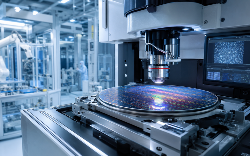
Atomic force microscopy measures a surface by moving an extremely small probe across it. The process is conceptually similar to a record-player needle following the contours of a vinyl record, although semiconductor measurements are performed at dramatically smaller dimensions and with far greater precision.
Traditional optical measurement systems encounter limitations as semiconductor features become smaller than the wavelengths of light used to examine them. Atomic force microscopy can measure physical structures directly, allowing chipmakers to inspect dimensions that are difficult to resolve using conventional optical techniques.
The historical weakness of atomic force microscopy has been speed. A highly accurate instrument is commercially limited if it cannot complete measurements quickly enough for a high-volume semiconductor factory. Nearfield Instruments has developed parallel scanning technology intended to combine atomic resolution with production-level throughput.
This is the central commercial proposition behind the company’s QUADRA platform. Nearfield Instruments is attempting to move atomic force microscopy from a specialist laboratory function into routine process control across advanced manufacturing lines.
Success would create meaningful switching costs. Semiconductor manufacturers do not casually replace process-control equipment after integrating it into production recipes, quality systems and yield-management procedures. Once qualified, an inspection platform can remain linked to a particular manufacturing process for years.
The qualification process is also a barrier to entry. Chipmakers must test whether a new metrology system can deliver consistent measurements without slowing production or damaging wafers. The long approval cycle can delay revenue, but it also protects suppliers after their technology is accepted.
Why are three-dimensional chip designs increasing demand for Nearfield Instruments’ metrology systems?
The semiconductor industry is no longer relying solely on shrinking two-dimensional features to improve performance. Manufacturers are increasingly building vertical structures, stacking components and connecting several chips through advanced packaging.
Nearfield Instruments has identified High Numerical Aperture Extreme Ultraviolet lithography, Gate-All-Around transistors, Complementary Field-Effect Transistor architectures and hybrid-bonded three-dimensional integration as important applications for its technology. Each architecture introduces structures that are taller, narrower, more complex or more difficult to inspect using conventional methods.
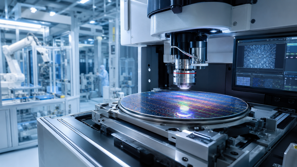
Gate-All-Around transistor designs require precise control around nanoscale channels. High Numerical Aperture Extreme Ultraviolet lithography increases patterning precision but also raises the cost of manufacturing errors. Hybrid bonding requires extremely accurate alignment and surface preparation when separate semiconductor components are connected.
These changes expand the number of dimensions manufacturers must measure. A chipmaker may need information about the top surface, sidewalls, depth, shape and alignment of a structure rather than a single width measurement.
Nearfield Instruments introduced a sidewall imaging capability for its platform in 2026, reflecting this move toward more complex three-dimensional process control. The development allows chip manufacturers to inspect vertical surfaces that become increasingly important as transistor and memory structures extend upward rather than merely becoming narrower.
Advanced packaging creates another opportunity. Artificial intelligence systems frequently combine processors, memory and interconnect technologies within one package. A small alignment error between components can reduce performance or render the package unusable, increasing the value of accurate inspection.
How will Nearfield Instruments use $380 million to move from technology validation to global manufacturing scale?
Nearfield Instruments intends to expand production capacity and improve the productivity of its manufacturing operations. Management is responding to customer demand by attempting to reduce equipment lead times and deliver more systems without compromising reliability.
Scaling semiconductor equipment manufacturing is different from expanding a software platform. Nearfield Instruments must source precision components, assemble sophisticated machines, conduct extensive testing and support each system after installation.
Growth therefore requires working capital as well as research spending. Components may need to be ordered months before a completed system is delivered and paid for. A rapid increase in orders can consume cash even when the underlying business is commercially healthy.
The company also plans to create Applications Centers of Excellence in major semiconductor regions. These centres can help customers test measurement methods, adapt equipment to specific manufacturing processes and evaluate new applications before installing systems in production facilities.
Customer support is equally important. A metrology system operating inside an advanced semiconductor factory cannot remain unavailable for long periods. Nearfield Instruments must provide engineers, spare parts, software updates and technical assistance near its customers.
The company already maintains a presence in the Netherlands, the United States, Japan, South Korea, Singapore and Taiwan, placing it near many of the world’s largest semiconductor manufacturing and research clusters.
The funding should allow Nearfield Instruments to build a more durable global service organisation before its installed base becomes too large to support from Rotterdam. That expansion may reduce margins in the near term, but weak support would create a far greater risk by slowing customer adoption.
What does the investor group reveal about the strategic importance of semiconductor metrology?
The Series D combines traditional institutional capital with sovereign and industrially focused investors. Fidelity Management & Research Company led the round, while Temasek, Qatar Investment Authority, Invest-NL and other existing investors participated.
This mix reflects the changing nature of semiconductor investment. Chip equipment companies are no longer viewed only as specialised technology suppliers. They are increasingly treated as strategic infrastructure because access to manufacturing tools can influence national computing capacity, industrial competitiveness and defence capability.
Temasek’s participation provides a link to Singapore, one of Asia’s major semiconductor manufacturing and research centres. Qatar Investment Authority adds a sovereign investor seeking exposure to the expanding artificial intelligence infrastructure market. Invest-NL reflects the Netherlands’ interest in retaining and scaling domestic semiconductor expertise.
Walden Catalyst Ventures also brings a direct semiconductor network. The venture firm was founded by industry executives with experience across global chip companies and has supported Nearfield Instruments through earlier growth stages.
The diversity of the investor base can help Nearfield Instruments enter new markets and build relationships. However, it also creates high expectations. A $1.6 billion valuation requires the company to convert technical relevance into sustained equipment sales, recurring service revenue and global customer adoption.
The round’s oversubscription suggests capital demand exceeded the shares available, but investor enthusiasm does not eliminate execution risk. Semiconductor equipment companies remain exposed to lengthy customer qualification cycles and abrupt changes in capital spending.
Can Nearfield Instruments challenge KLA in a semiconductor inspection market dominated by incumbents?
KLA Corporation is the dominant global provider of semiconductor process-control and inspection equipment. Its scale, installed base and relationships with major chip manufacturers create a formidable competitive barrier for any emerging supplier.
Nearfield Instruments does not need to replace KLA across every category to build a valuable business. Semiconductor factories use multiple measurement technologies because no single system can inspect every material, surface and structure.
The company’s opportunity lies in measurements where conventional optical or electron-based techniques struggle to provide the required combination of resolution, three-dimensional information and production speed. Nearfield Instruments can become a complementary supplier before attempting to expand into a broader share of the process-control budget.
Its European base also places the business within a powerful equipment ecosystem. The Netherlands is home to ASML Holding, ASM International and BE Semiconductor Industries, giving Nearfield Instruments proximity to engineering talent, specialised suppliers and semiconductor customers.
The presence of those companies does not guarantee success, but it creates an industrial environment where highly specialised equipment businesses can recruit experienced engineers and collaborate across complex production challenges.
Nearfield Instruments has already identified Samsung Electronics as a customer and previously disclosed multiple orders from an unnamed United States customer. These relationships provide evidence that the company’s technology has progressed beyond laboratory testing, although the concentration and financial value of individual customer contracts remain undisclosed.
The central competitive test will be repeat orders. A first installation can reflect experimentation. Multiple systems deployed across several production lines would indicate that Nearfield Instruments has become part of a chipmaker’s standard process-control strategy.
Does the $1.6 billion valuation suggest Nearfield Instruments is preparing for an IPO?
Nearfield Instruments previously indicated that it was considering a stock market listing in 2027 or by 2028 at the latest, subject to market conditions. The $380 million Series D gives the company sufficient private capital to expand before making that decision.
The financing can support an eventual IPO in two ways. First, it allows Nearfield Instruments to increase revenue and build a larger installed base before public investors assess the company. Second, the participation of Fidelity Management & Research Company introduces an investor with extensive experience evaluating listed technology companies.
However, the round could also reduce the urgency of an IPO. Nearfield Instruments now has substantial capital to fund manufacturing and international expansion without immediately accepting quarterly reporting requirements or public-market volatility.
The $1.6 billion private valuation will become a reference point for any future listing. Nearfield Instruments must demonstrate enough growth to justify a higher public valuation after allowing for dilution, market conditions and the cyclical nature of semiconductor spending.
An IPO would also require greater financial transparency. Public investors would expect information about revenue, gross margins, order backlog, customer concentration, research spending and cash flow.
The company has disclosed strong demand but not detailed financial performance. That is normal for a private business, yet the transition from a technology story to a public investment case will require considerably more evidence.
The financing therefore looks pre-IPO in scale, but it should not be treated as confirmation of an imminent listing. The stronger interpretation is that Nearfield Instruments has purchased the flexibility to choose its timing.
What execution risks could prevent Nearfield Instruments from converting demand into durable growth?
The semiconductor cycle remains the most obvious external risk. Artificial intelligence investment is currently supporting demand for advanced equipment, but chipmakers can reduce capital spending quickly when inventories rise or economic conditions weaken.
Nearfield Instruments is also exposed to customer concentration. Only a limited number of companies operate the most advanced semiconductor manufacturing facilities, which means losing a qualification programme or experiencing a customer delay could materially affect growth.
Manufacturing execution presents another risk. Precision equipment must be assembled consistently as production volumes increase. Quality problems that are manageable at low volume can become expensive when the company is delivering systems across several countries.
Supply-chain availability may also constrain expansion. Semiconductor equipment contains specialised mechanical, optical, electronic and software components that cannot always be replaced easily when suppliers experience delays.
Nearfield Instruments must continue investing in research while scaling production. Focusing too heavily on current orders could allow competitors to close the technology gap, while excessive product development could divert resources from delivery and customer support.
The company’s valuation creates pressure of its own. Investors funding a $1.6 billion private company will expect a meaningful return, which may encourage rapid growth, acquisitions or an eventual IPO. Management must avoid allowing fundraising success to dictate operational decisions.
The largest risk may be that demand develops more slowly than expected. Chipmakers can recognise the technical value of a new inspection tool while taking years to qualify and deploy it across production. Nearfield Instruments has raised enough capital to support that transition, but money cannot make semiconductor qualification cycles magically less patient.
What should investors watch after Nearfield Instruments completes its Series D funding?
Production expansion will be the first indicator. Nearfield Instruments needs to demonstrate that the capital reduces lead times and increases deliveries rather than merely expanding facilities and headcount.
The second indicator will be customer diversification. Additional disclosed orders from the United States, Taiwan, South Korea or Japan would reduce dependence on a small number of advanced chip manufacturers.
Repeat purchases will be particularly important because they indicate that customers are moving from evaluation to production deployment. Service and software revenue generated from an expanding installed base could also improve the stability of the business.
Applications centres should provide another measure of progress. Their value will depend on whether they accelerate customer qualification, create new measurement recipes and lead to equipment orders.
Investors should also monitor whether Nearfield Instruments extends its technology beyond advanced logic chips. The company has previously identified growing interest from memory manufacturers and producers of semiconductors used in vehicles and power infrastructure.
Finally, any renewed IPO guidance will reveal whether the Series D is intended as the final major private financing. A listing in 2027 or 2028 would give public investors access to one of Europe’s few emerging semiconductor equipment challengers.
Key takeaways on what Nearfield Instruments’ funding means for AI chip manufacturing
- Nearfield Instruments has raised $380 million at a $1.6 billion valuation in the largest deep-tech funding round completed in the Netherlands.
- Fidelity Management & Research Company led the oversubscribed Series D, with sovereign and institutional investors supporting the transaction.
- The company will use the capital to increase manufacturing capacity, shorten lead times and expand global customer support.
- Nearfield Instruments’ atomic force microscopy systems measure semiconductor structures at dimensions that challenge conventional optical techniques.
- Artificial intelligence processors and three-dimensional chip architectures are increasing the need for more accurate process control.
- The commercial opportunity depends on helping chipmakers improve production yield rather than merely providing higher-resolution images.
- KLA Corporation remains the dominant process-control supplier, but Nearfield Instruments can grow by targeting difficult measurement applications.
- Samsung Electronics and an unnamed United States manufacturer have previously placed orders, providing evidence of customer adoption.
- The $1.6 billion valuation increases expectations around repeat sales, manufacturing execution and future profitability.
- Nearfield Instruments’ earlier IPO ambition for 2027 or 2028 remains a potential next step, although the new funding reduces pressure to list quickly.
Share this:
Discover more from Business-News-Today.com
Subscribe to get the latest posts sent to your email.