




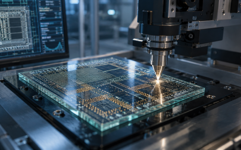
Intel Corporation (NASDAQ: INTC) and Chinese precision manufacturer Lens Technology (SEHK: 6613; SZSE: 300433) have announced a strategic collaboration on advanced semiconductor packaging, specifically targeting glass substrate technology for artificial intelligence and data centre workloads. The tie-up, announced jointly from Santa Clara and Changsha on July 24, 2026, will explore through-glass via processes, high-precision laser processing and metal-filled via deposition, all of which sit at the core of the industry’s most contested advanced-packaging bet. According to Lens Technology’s own exchange filing, the arrangement is a memorandum of understanding signed by its wholly owned subsidiary Lens International (HK) Limited, with most provisions non-binding and valid for one year. That framing is important, because it separates a strategic signal from a committed commercial supply arrangement. The central tension is straightforward, whether Intel can convert a widening ecosystem of glass-substrate partners into a technology that actually scales before its 2030 packaging roadmap window closes.
What did Intel and Lens Technology actually agree, and how binding is the arrangement?
The Intel announcement is written in the vocabulary of a strategic collaboration, but the underlying document is narrower. Lens Technology told the Hong Kong Stock Exchange that the memorandum covers exploratory cooperation across glass substrate via formation, high-precision laser processing and metal-filled via deposition, with any concrete engineering validation or volume production to be governed by separate agreements. Most provisions are non-binding and effective for one year. Beyond through-glass via, the two companies said they may also examine structural components and modules for AI PCs, high-reliability thermal solutions for data centre servers, and hardware for embodied AI robotics and edge computing.
For readers used to interpreting Intel headlines through the lens of foundry customer wins, this is a different category of announcement. It is not a signed supply contract, a wafer commitment, or a joint venture. It is a framework that gives both sides the option to move to binding engineering validation, subject to further negotiation. That distinction matters commercially. Intel has spent much of 2026 trying to demonstrate that its advanced packaging and foundry roadmap can attract external validation, and a named glass substrate partner is a credibility marker. However, the market should not confuse a framework MOU with a qualified, revenue-generating supply relationship.
Why is through-glass via the technical prize, and why is Lens Technology in the frame?
Advanced packaging has become the industry’s principal answer to the slowing economics of monolithic transistor scaling, and glass core substrates are the material bet inside that shift. Compared with the woven-glass organic substrates that have carried most of the semiconductor industry for decades, glass core offers higher dimensional stability, better electrical properties, and the mechanical flatness required for the next generation of larger, chiplet-heavy packages used in AI accelerators. Intel first added glass substrates to its advanced packaging roadmap in 2023, framing the technology as central to its target of scaling one trillion transistors on a package by 2030. The company debuted a sample combining its EMIB 2.5D bridge technology with a glass core substrate at NEPCON Japan in January 2026.
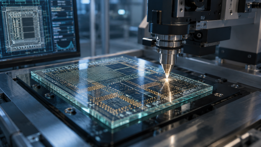
The unresolved bottleneck is the through-glass via itself. To carry electrical signals vertically through a glass substrate, manufacturers must drill and align microscopic vias through a brittle material at consistent yield and reliability. Every glass substrate contender, including SKC’s Absolics in Georgia, Samsung Electro-Mechanics, LG Innotek and TSMC’s panel-level packaging effort, is racing the same yield problem on timelines that mostly land between 2027 and 2030. That is exactly where Lens Technology fits. Founded in Changsha in 1993, Lens Technology built its reputation as the world’s largest supplier of consumer-electronics precision cover glass, sapphire, ceramics and metal structural parts, with 2024 revenue of about RMB 69.9 billion. Its industrial capability set, particularly ultra-precision laser drilling on glass at scale, is directly relevant to the TGV process step. Intel is effectively renting access to that capability at pilot scale, rather than trying to develop it entirely inside its own manufacturing organisation.
How does this fit into Intel’s foundry and capital-allocation strategy under Lip-Bu Tan?
The announcement lands in the middle of the most closely watched phase of Intel’s turnaround. Chief executive Lip-Bu Tan took over in March 2025 and has spent the intervening period trying to demonstrate three things: that the Intel 18A process node can reach economic yield, that Intel Foundry can attract external customers, and that the balance sheet can absorb the cost of both while restructuring proceeds. Q2 2026 revenue of $16.1 billion was up about 25 percent year on year, the fastest growth in more than fifteen years, and adjusted earnings per share of 42 cents doubled consensus. Third-quarter revenue guidance of about $16.3 billion was around 8 percent above analyst expectations.
Yet the market reaction was punitive. Intel shares fell 7.9 percent on July 24, 2026, closing at $92.32 despite the beat, as investors focused on the disclosure that external foundry revenue remains a small share of the total and that Intel Foundry is losing at a run rate of roughly $8 billion annually. Capital spending for 2026 was raised to $20 billion. Against that backdrop, the Lens Technology framework is a low-cost strategic signal. It does not commit capital, it does not add a foundry customer, and it does not de-risk the 18A ramp. What it does is add an external partner to the glass substrate part of the roadmap, at a moment when Tan has been explicitly trying to broaden Intel’s ecosystem rather than defend a fully vertical model. Coming days after Fortinet was disclosed as the first named external foundry customer, and alongside earlier equity investments from NVIDIA and SoftBank, the Lens Technology tie-up fits a pattern of partnership breadth over depth.
What does Lens Technology gain, and where is the risk for its investors?
For Lens Technology, the strategic logic runs in the opposite direction. The company has long been dependent on smartphone and consumer electronics cover glass, a category where growth has flattened and pricing pressure from Chinese peers is intense. Its 2025 secondary listing on the Hong Kong Stock Exchange, priced at HKD 18.18 per share and raising about HKD 4.8 billion, was explicitly positioned as funding for global expansion and diversification into higher-value adjacencies including smart vehicles and, now, semiconductor packaging. Extending its precision glass, laser and structural capabilities into the semiconductor substrate value chain represents a durable margin opportunity, if the qualification cycles convert.
The commercial risk sits in exactly the same place as the opportunity. Customer qualification cycles for advanced packaging materials typically run 18 to 36 months, and Intel’s own commercial deployment of glass substrates is targeted for late in the decade. Any revenue contribution to Lens Technology from this arrangement is unlikely to appear in the near-term earnings line. The share price context reflects that longer horizon. Lens Technology shares in Hong Kong were trading at HKD 22.94 at a recent close, inside a 52-week range of HKD 15.68 to HKD 33.94, with a Bloomberg-tracked consensus 12-month target near HKD 28. DBS initiated coverage with a Buy rating in June 2026. Business News Today did not identify a widely published broker note attributing near-term earnings uplift to the Intel arrangement, which is consistent with the non-binding framework language in the exchange filing.
Does the US-China semiconductor policy environment change how this collaboration should be read?
A US technology company signing a strategic advanced-packaging framework with a Chinese partner, at a time when US semiconductor export controls have progressively tightened, is worth examining on its own terms. The specific area of cooperation is instructive. Through-glass via processing, precision laser drilling and glass substrate metallisation are packaging and materials capabilities, not front-end wafer fabrication technologies or advanced logic process nodes. They fall outside the categories most tightly restricted by current US export control regimes, which have focused on advanced logic tooling, EUV lithography and high-bandwidth memory intended for AI training clusters in China.
However, the political sensitivity of any US chip company deepening its ties into the Chinese electronics supply chain is unlikely to disappear. Investors should watch whether the arrangement stays confined to research collaboration and materials sourcing, whether it evolves into a co-manufacturing footprint, and whether any component of the collaboration eventually touches product areas the US Commerce Department could later reclassify. The one-year, non-binding character of the memorandum gives both sides room to adjust scope if the policy environment shifts.
What evidence will show whether this collaboration is more than a signal?
For Intel investors, the meaningful proof points will not be in press releases. They will be in three sequential milestones. First, whether the non-binding MOU is followed within the next twelve months by a binding engineering validation agreement, which would move the relationship from optionality to commitment. Second, whether Intel’s advanced packaging roadmap communications through 2027 and 2028 begin to name specific supply partners for the glass substrate value chain, which would suggest that TGV yield is progressing at a pace consistent with the 2030 target. Third, whether Intel Foundry’s external revenue mix continues to broaden beyond its first named customer, Fortinet, and whether external revenue moves from around five percent of foundry revenue toward a level that visibly offsets the current loss run rate.
For Lens Technology investors, the equivalent tests are whether the arrangement translates into a semiconductor supply-chain revenue line in future filings, whether the company invests further capital in laser and TGV process capacity beyond its existing base in Changsha, and whether other advanced packaging incumbents, including TSMC and its glass substrate ecosystem, add Lens Technology to their qualified supplier lists.
What has improved for Intel, and what remains unresolved?
The Lens Technology framework marginally improves the credibility of Intel’s glass substrate roadmap by adding a large, industrially competent external partner to a technology stack that has so far been discussed largely in Intel-internal terms. It does not change the near-term profitability of Intel Foundry, it does not resolve the through-glass via yield problem, and it does not commit either party to volume production. The unresolved question is the same one facing the broader glass substrate industry, whether the transition from organic to glass core substrates arrives at the price and yield points the AI packaging market requires, before organic substrate innovation extends its own commercial life. The next measurable proof point for this specific arrangement is whether it survives its one-year non-binding window and converts into a binding engineering validation agreement. Everything downstream of the AI packaging thesis, from Intel’s 2030 transistor target to Lens Technology’s diversification story, ultimately depends on that step.
Key takeaways: What the Intel and Lens Technology MOU signals about the AI packaging race
- Intel Corporation and Lens Technology announced a strategic collaboration on advanced semiconductor packaging, focused on glass substrate technology for AI and data centre workloads.
- The Lens Technology exchange filing clarifies the arrangement is a mostly non-binding memorandum of understanding, signed by wholly owned subsidiary Lens International (HK) Limited, with a one-year term.
- Scope covers through-glass via formation, high-precision laser processing and metal-filled via deposition, plus potential collaboration on AI PC components, data centre thermal solutions, robotics hardware and edge computing.
- Through-glass via yield remains the industry’s hardest unsolved step in the glass substrate transition, with commercial deployment across the sector targeted between 2027 and 2030.
- Intel’s advanced packaging roadmap has included glass substrates since 2023, with the company targeting one trillion transistors on a package by 2030 and demonstrating an EMIB plus glass core sample at NEPCON Japan in January 2026.
- Intel Foundry is losing at a run rate of roughly $8 billion annually and reported external customer revenue at around 5 percent of foundry revenue in Q2 2026, despite total company revenue growth of 25 percent to $16.1 billion.
- Intel shares fell 7.9 percent to $92.32 on the earnings session preceding this announcement, reflecting investor focus on foundry economics rather than headline revenue growth.
- Lens Technology gains a diversification pathway from consumer electronics cover glass into the higher-value semiconductor substrate supply chain, subject to typical 18 to 36 month qualification cycles.
- The US-China policy backdrop is a real but currently secondary consideration, as the cooperation sits in packaging and materials rather than front-end logic or EUV-linked capabilities restricted by export controls.
- The most important near-term test is whether the non-binding MOU is followed within twelve months by a binding engineering validation agreement between Intel and Lens Technology.
Discover more from Business-News-Today.com
Subscribe to get the latest posts sent to your email.