


Why is Gigaphoton expanding its field service operations in Kyushu amid Japan’s semiconductor investment wave?
Gigaphoton Inc., the Japanese lightsource manufacturer for semiconductor lithography systems, officially completed its new Kyushu office on June 27, 2025, marking a major strategic expansion aimed at reinforcing its field support infrastructure in southern Japan. The new facility significantly increases Gigaphoton’s support capacity—by threefold—amid escalating demand from chip fabrication facilities across the Kyushu region.
Founded in 2000 and headquartered in Oyama, Tochigi Prefecture, Gigaphoton has built a global reputation for its laser lightsource systems used in semiconductor lithography. The manufacturer plays a vital role in the chip production value chain by ensuring uptime and reliability for lithography tools at customer fabs, many of which are clustered across Japan. This latest move to fortify its Kyushu operations aligns with both national industrial policy and private sector momentum to decentralize semiconductor investments away from traditional tech hubs.
Institutional observers note that Japan’s semiconductor ecosystem is experiencing a renewed infrastructure push, driven by domestic reshoring incentives, geopolitical supply chain strategies, and multi-billion-dollar investments by companies such as TSMC, Rapidus, and Sony. As semiconductor fabs multiply across regional bases like Kyushu, the need for proximity service and parts support has grown sharply.
Gigaphoton’s Kyushu expansion offers a clear signal of how upstream equipment providers are adapting operationally to meet this anticipated surge in customer requirements.
What does the Kyushu office completion mean for Gigaphoton’s semiconductor field services network?
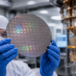
The newly completed Kyushu site is now Gigaphoton’s first fully-owned support office in Japan outside of its headquarters in Oyama. Designed to function not just as a dispatch hub but also as a module servicing and training center, the office spans two stories with a total floor area of 1,112.66 square meters.
This facility will serve as a critical operational node for servicing excimer laser lightsource systems, offering localized support to customers in Kyushu’s burgeoning chip manufacturing corridor. The Kyushu office is expected to function across three core areas: rapid-response field service operations, repair and maintenance of supply modules, and ongoing customer training and technical education.
By consolidating these service pillars under one roof, Gigaphoton is poised to deliver faster turnaround times and greater operational reliability to semiconductor fabs across southern Japan. This is especially crucial for maintaining tight lithography uptime metrics at fabrication plants, where even minor disruptions in lightsource systems can lead to costly wafer production delays.
In essence, the new Kyushu office acts as a logistics and knowledge hub for Gigaphoton’s support network, embedding higher levels of technical capacity directly in proximity to customer fabs.
How does this expansion tie into broader Japanese semiconductor localization trends?
Japan’s government-led semiconductor renaissance has fueled a flurry of regional investment, particularly in Kyushu. The region has emerged as a central node in Japan’s national semiconductor strategy, hosting advanced packaging, memory, and logic fabrication projects by both domestic and international players.
Key multinationals such as Taiwan Semiconductor Manufacturing Company (TSMC) have committed to constructing new fabs in Kumamoto, while Rapidus—Japan’s homegrown logic foundry champion—is targeting advanced node development with international technology partners. Against this backdrop, equipment manufacturers like Gigaphoton are recalibrating their footprints to align with where semiconductor capacity is physically being built.
The Japanese lightsource developer has maintained a presence in Kyushu since the year 2000 through a smaller support office. However, the exponential increase in fab investments and service demands has triggered the need for a vastly upgraded physical presence. This expansion not only fulfills that operational need but signals long-term confidence in Kyushu’s role as a semiconductor cluster.
Industry sentiment suggests that Gigaphoton’s move will serve as a bellwether for other upstream equipment and service providers to follow suit with localized expansion strategies.
What has Gigaphoton signaled about its long-term commitment to service-led differentiation?
According to Gigaphoton President and CEO Tatsuo Enami, the company’s long-term growth strategy hinges on “enhancing service capacity worldwide” to support the evolving requirements of the semiconductor industry. The Kyushu office is positioned as a template for future regional expansions, built to support both technical service operations and knowledge transfer through training.
Gigaphoton emphasizes open, sustained communication with its customer base as a core differentiator in its service philosophy. The company maintains that by offering real-time regional support and integrating supply module servicing and training under one roof, it will be better equipped to meet the reliability standards demanded by next-generation fabs.
While not publicly listed, Gigaphoton’s operational growth strategies are closely watched by institutional stakeholders given the critical importance of photolithography subsystems in semiconductor yield management.
Institutional investors and ecosystem participants see this move as part of a broader shift where support infrastructure is being scaled in anticipation of sustained demand, rather than reacting to bottlenecks.
What is the future outlook for Gigaphoton’s domestic and global field service footprint?
Analysts expect that Gigaphoton will replicate the Kyushu model in other semiconductor growth markets, both domestically and overseas. With chipmaking capacity continuing to globalize beyond traditional centers, the need for near-site service hubs with in-house training and supply part logistics will only grow.
In Japan, additional expansions may target regions like Hokkaido and Chubu, where new government-backed fabrication projects are being negotiated. Internationally, the lightsource maker has existing service operations in key markets such as Taiwan, China, South Korea, and the United States. The success of the Kyushu model could influence how those operations are scaled in the future.
Furthermore, as semiconductor technologies advance toward EUV (extreme ultraviolet) lithography, the complexity of lightsource systems—and the required service expertise—will grow. This reinforces the need for robust field infrastructure and technician upskilling programs, both of which the new Kyushu facility aims to institutionalize.
Analysts believe that Gigaphoton’s blend of service localization and training-focused investments may help it maintain or grow its market share in a competitive supplier landscape dominated by global players.
Share this:
Discover more from Business-News-Today.com
Subscribe to get the latest posts sent to your email.