


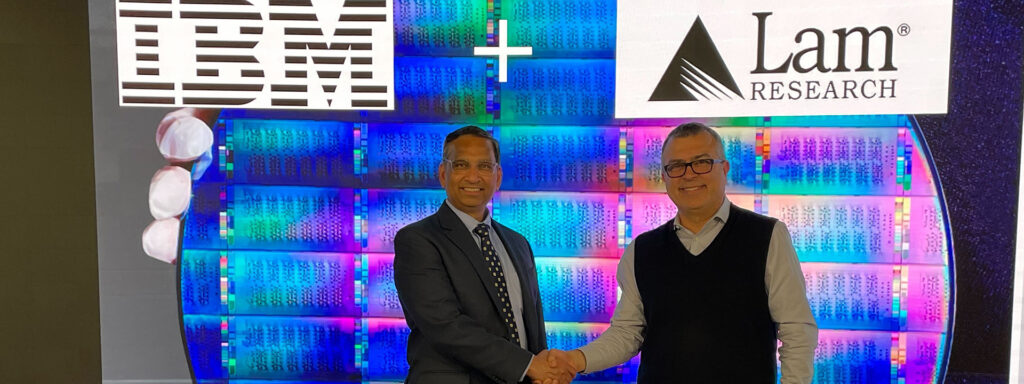
IBM Corporation and Lam Research Corporation have announced a new five-year collaboration designed to push semiconductor logic scaling into the sub-1nm era, with joint research focusing on advanced materials, next-generation fabrication processes, and High-NA extreme ultraviolet lithography techniques. The partnership builds on more than a decade of joint development work between the two companies and aims to address the increasingly complex technological challenges that now define the future of advanced semiconductor manufacturing.
The announcement signals that the semiconductor industry is entering a phase where traditional transistor shrinking is no longer sufficient to maintain performance gains. Instead, progress will increasingly depend on coordinated advances across multiple manufacturing disciplines including materials science, lithography integration, etch technology, deposition systems, device architecture design, and packaging innovations. For IBM Corporation, the collaboration reinforces its position as a leading research hub for next-generation chip technologies. For Lam Research Corporation, the agreement strengthens its strategic role in the process technologies that enable increasingly complex semiconductor devices.
At its core, the collaboration aims to develop practical manufacturing pathways for future logic nodes that extend beyond current roadmaps. The work will be conducted primarily at the NY Creates Albany NanoTech Complex in New York, where IBM Corporation maintains one of the world’s most advanced semiconductor research facilities. Lam Research Corporation will contribute its process technology expertise and fabrication equipment platforms to help develop and validate complete manufacturing flows capable of supporting sub-1nm device architectures.
Why the IBM Corporation and Lam Research Corporation partnership reflects a broader shift in semiconductor innovation
The semiconductor industry has historically advanced through predictable transistor scaling cycles, often described through Moore’s Law. However, the technical barriers associated with continued miniaturization have increased dramatically in recent years. As transistors approach atomic dimensions, improvements in chip performance increasingly depend on innovations that go far beyond traditional lithographic patterning.
The collaboration between IBM Corporation and Lam Research Corporation highlights how semiconductor progress is now driven by the integration of multiple technologies rather than by a single breakthrough. Future nodes require coordinated development of new materials, advanced patterning strategies, and entirely new device structures that can sustain performance gains while maintaining manufacturability.
One of the central themes of the partnership is the development of new materials that can support next-generation transistor structures. As device architectures become increasingly complex, traditional semiconductor materials often struggle to deliver the electrical characteristics required for high performance and energy efficiency. Researchers are therefore exploring new materials that can provide improved conductivity, reduced resistance, and greater thermal stability within extremely small geometries.
Another key focus area is the development of fabrication processes capable of handling these advanced materials. Semiconductor manufacturing involves hundreds of precisely controlled process steps, and even small changes in materials or device architecture can require significant adjustments to etch, deposition, and patterning technologies. By working together, IBM Corporation and Lam Research Corporation aim to create integrated process flows that allow these new technologies to transition from laboratory demonstrations to practical manufacturing techniques.
How High-NA EUV lithography could shape the next generation of advanced semiconductor nodes
High numerical aperture extreme ultraviolet lithography represents one of the most important enabling technologies for future semiconductor scaling. Conventional EUV lithography has already transformed the semiconductor industry by allowing chip manufacturers to print extremely small features on silicon wafers. However, as the industry moves toward sub-1nm nodes, even EUV systems must evolve to maintain the resolution required for advanced chip architectures.
High-NA EUV lithography increases the numerical aperture of the optical system used during the lithography process, enabling higher resolution patterning on semiconductor wafers. This improvement allows chip manufacturers to create smaller and more precise features, which in turn supports higher transistor densities and improved performance.
Despite its potential, High-NA EUV lithography introduces several technical challenges that extend far beyond the lithography tool itself. The resist materials used during patterning must be capable of handling higher photon energies while maintaining pattern fidelity. Additionally, the patterns created during the lithography process must be transferred accurately into the underlying device layers through advanced etch processes.
IBM Corporation and Lam Research Corporation plan to address these challenges by developing integrated lithography and pattern transfer solutions. Their collaboration will focus on technologies such as dry resist processing, advanced etch platforms, and deposition systems designed to support increasingly complex device structures. These technologies will be tested in combination with new transistor architectures including nanosheet and nanostack devices, which represent some of the most promising candidates for future logic nodes.
Why advanced materials and process integration are becoming central to the future of semiconductor scaling
The semiconductor industry’s shift toward three-dimensional device structures has fundamentally changed how chips are manufactured. In earlier generations of semiconductor technology, performance improvements primarily came from shrinking planar transistors. Today, however, chip designers rely on complex structures that extend vertically through multiple layers of materials.
These structures require highly precise fabrication techniques capable of depositing and removing materials with atomic-scale accuracy. Lam Research Corporation specializes in many of the tools used during these steps, including etch platforms and deposition systems that enable manufacturers to construct intricate semiconductor devices.
The collaboration with IBM Corporation allows Lam Research Corporation to participate in the early development of new process technologies that may define future semiconductor nodes. By working closely with IBM researchers, Lam engineers can explore how their equipment platforms can be adapted to support next-generation device architectures.
The partnership will also focus on backside power delivery technologies, which are expected to play an increasingly important role in future chip designs. Backside power delivery allows power connections to be routed through the backside of a semiconductor wafer rather than through the same layers used for signal routing. This approach can improve chip performance and reduce electrical interference, but it requires new manufacturing techniques that are still under development.
By integrating these innovations into a unified process flow, IBM Corporation and Lam Research Corporation aim to demonstrate that sub-1nm semiconductor manufacturing can be both technically feasible and economically viable.
How the IBM Corporation and Lam Research Corporation alliance strengthens the Albany semiconductor research ecosystem
The NY Creates Albany NanoTech Complex has become one of the most important semiconductor research centers in the world. The facility hosts collaborations between industry leaders, academic institutions, and government organizations working on next-generation semiconductor technologies.
IBM Corporation has long played a central role in this ecosystem, using the Albany facility as a hub for research into advanced transistor architectures and semiconductor manufacturing processes. The partnership with Lam Research Corporation reinforces the importance of this facility as a location where early-stage semiconductor innovations can be developed and tested before moving toward commercial manufacturing.
The Albany research center allows companies to experiment with new manufacturing technologies without the cost and risk associated with full-scale production lines. This environment makes it possible to explore emerging process technologies that may eventually be adopted by large semiconductor foundries.
The collaboration between IBM Corporation and Lam Research Corporation therefore has implications beyond the two companies themselves. Breakthroughs achieved through this partnership could eventually influence manufacturing strategies across the global semiconductor industry.
Why the collaboration between IBM Corporation and Lam Research Corporation matters for the AI era of computing
The rapid expansion of artificial intelligence applications has dramatically increased demand for advanced semiconductor technology. AI workloads require enormous computational resources, which in turn depend on increasingly powerful and energy-efficient chips.
Sub-1nm logic scaling represents one possible path toward delivering the performance improvements needed for next-generation AI systems. By increasing transistor density and improving energy efficiency, advanced semiconductor nodes can support the massive computing infrastructure required for modern machine learning models.
IBM Corporation has positioned itself as a leader in enterprise AI systems and hybrid cloud infrastructure. Continued investment in semiconductor research allows the company to maintain a role in shaping the hardware technologies that underpin these platforms.
For Lam Research Corporation, the AI boom has reinforced the importance of advanced semiconductor manufacturing equipment. As chip architectures become more complex, semiconductor manufacturers require increasingly sophisticated fabrication tools capable of supporting new materials and process technologies.
The partnership therefore aligns with broader industry trends that link semiconductor innovation directly to the growth of artificial intelligence and high-performance computing.
Investor sentiment around IBM Corporation and Lam Research Corporation reflects long-term technology positioning
Market reactions to the collaboration announcement have been relatively measured, which reflects the long-term nature of semiconductor research partnerships. Unlike product launches or large capital investments, research collaborations typically influence industry development over multiple years rather than producing immediate revenue impacts.
IBM Corporation remains a diversified technology company with major operations in hybrid cloud computing, consulting services, and enterprise software. Semiconductor research supports the company’s broader technological credibility but does not directly drive near-term financial performance.
Lam Research Corporation, on the other hand, operates directly within the semiconductor equipment market, where demand is closely linked to chip manufacturing investments. As semiconductor nodes become more complex, the number of fabrication steps required to produce advanced chips tends to increase. This trend can benefit equipment suppliers whose tools enable those additional process steps.
The collaboration with IBM Corporation may therefore strengthen Lam Research Corporation’s long-term positioning within the semiconductor manufacturing ecosystem. Participation in early-stage process development allows the company to align its technology roadmap with emerging manufacturing requirements.
What the IBM Corporation and Lam Research Corporation partnership reveals about the future of semiconductor scaling
The agreement between IBM Corporation and Lam Research Corporation highlights an important shift in how semiconductor progress will be achieved in the coming decades. Future scaling will depend less on isolated breakthroughs and more on coordinated advances across the entire manufacturing ecosystem.
Materials science, lithography, etch technologies, deposition processes, and device architecture design must now evolve together in order to maintain the pace of semiconductor innovation. This collaborative approach reflects the growing complexity of chip manufacturing and the enormous technical challenges associated with continued transistor scaling.
If successful, the research conducted through this partnership could help establish new manufacturing pathways for semiconductor devices that extend beyond current technology nodes. Such progress would support the continued development of advanced computing systems used in artificial intelligence, cloud infrastructure, and high-performance computing environments.
For the semiconductor industry, the collaboration represents another step toward redefining what Moore’s Law means in the modern era. Rather than relying solely on smaller transistors, future performance improvements will emerge from deeper integration between materials innovation, device architecture design, and advanced manufacturing technologies.
The partnership between IBM Corporation and Lam Research Corporation therefore reflects not only the next stage of semiconductor scaling but also the increasingly collaborative nature of technological progress within one of the world’s most strategically important industries.
Key takeaways from the IBM Corporation and Lam Research Corporation collaboration on sub-1nm semiconductor technology
- IBM Corporation and Lam Research Corporation have launched a five-year research collaboration focused on advancing semiconductor logic scaling beyond current technology nodes toward the sub-1nm era.
- The partnership will concentrate on developing novel semiconductor materials, advanced fabrication processes, and High-NA extreme ultraviolet lithography integration to support future chip architectures.
- Research activities will primarily take place at the NY Creates Albany NanoTech Complex, where IBM Corporation operates one of the world’s leading semiconductor research environments.
- Lam Research Corporation will contribute advanced process technologies including etch and deposition platforms that are essential for building increasingly complex three-dimensional transistor structures.
- The collaboration aims to develop integrated manufacturing process flows capable of supporting nanosheet and nanostack transistor architectures as well as emerging backside power delivery technologies.
- High numerical aperture extreme ultraviolet lithography will play a central role in the research, enabling higher resolution patterning needed for future semiconductor nodes.
- The partnership reflects a broader shift within the semiconductor industry toward coordinated innovation across materials science, lithography, and process integration rather than relying solely on transistor shrinking.
- Advanced semiconductor technologies developed through this collaboration could support the growing computational demands of artificial intelligence systems and next-generation data center infrastructure.
- For IBM Corporation, the collaboration strengthens its role as a global semiconductor research leader even as the company focuses commercially on hybrid cloud and artificial intelligence platforms.
- For Lam Research Corporation, participation in early-stage process development reinforces its strategic position within the semiconductor manufacturing equipment ecosystem as chip fabrication complexity continues to increase.
Discover more from Business-News-Today.com
Subscribe to get the latest posts sent to your email.