


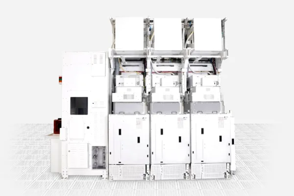
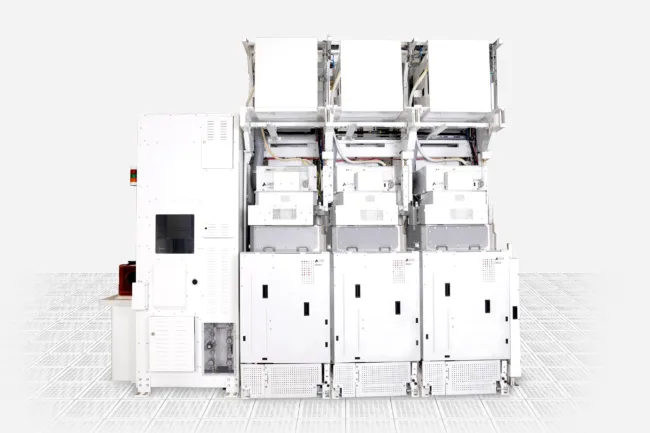
Lam Research Corporation has introduced two semiconductor manufacturing technologies designed to overcome critical scaling challenges in the chip industry. The newly launched Akara, an advanced conductor etch technology, and ALTUS Halo, the first molybdenum atomic layer deposition tool, represent significant advancements in chip manufacturing processes. As semiconductor devices continue to shrink while increasing in complexity, these innovations are set to redefine semiconductor fabrication technologies, offering superior precision, efficiency, and material control.
What Makes Akara a Breakthrough in Conductor Etch Technology?
Lam Research’s Akara marks a significant leap forward in conductor etch technology, addressing the critical need for ultra-precise etching processes in advanced semiconductor designs. The tool enables chipmakers to create intricate 3D transistor structures, such as gate-all-around (GAA) transistors, 6F2 DRAM, and 3D NAND devices, with unparalleled accuracy. Akara extends Lam Research’s two-decade leadership in plasma etch solutions, building on the success of its Kiyo etch platform, which has more than 30,000 chambers in production.
One of Akara’s key differentiators is its ability to provide angstrom-level etching precision, which is essential for forming high-aspect-ratio chip structures. Traditional plasma etch systems struggle to maintain uniformity and control at the atomic scale, but Akara overcomes these limitations through a combination of DirectDrive plasma technology, TEMPO plasma pulsing, and SNAP ion energy control. These innovations allow for rapid etch profile shaping, ensuring that chipmakers can execute highly controlled, defect-free etching processes for next-generation semiconductors.
How Does Akara Enhance Plasma Control for Advanced Chipmaking?
One of the most pressing challenges in semiconductor fabrication technologies is maintaining precise control over plasma etching processes to prevent defects and ensure repeatability in high-volume production. Akara addresses this issue with several proprietary innovations.
Lam Research’s DirectDrive plasma source is the first solid-state plasma generation technology, capable of achieving plasma responses 100 times faster than conventional systems. This speed allows for improved Extreme Ultraviolet (EUV) lithography patterning, reducing defects that typically arise from plasma instabilities. Additionally, TEMPO plasma pulsing fine-tunes plasma species to deliver unmatched etch selectivity and microloading performance, ensuring that structures maintain their intended geometries.
The SNAP ion energy control system enhances etch profile shaping, allowing chipmakers to achieve precisely tailored transistor architectures. This capability is particularly critical for high-aspect-ratio etching, where even slight variations in ion energy can lead to significant process deviations. By integrating these technologies into a single, high-performance system, Akara enables the production of smaller, faster, and more power-efficient chips.
What Role Does ALTUS Halo Play in Next-Generation Metallization?
Alongside Akara, Lam Research has unveiled ALTUS Halo, a revolutionary molybdenum atomic layer deposition (ALD) system designed to replace traditional tungsten-based metallization in chip manufacturing processes. As semiconductor devices become more complex, conventional metal deposition techniques are reaching their performance limits. Tungsten, which has long been the industry standard for nano-scale interconnects, presents challenges such as higher resistivity and the need for additional barrier layers to prevent electrical interactions.
ALTUS Halo overcomes these limitations by utilizing molybdenum, a metal that offers significantly lower resistivity at nano-scale dimensions. This innovation eliminates the need for barrier layers, reducing process complexity while improving chip speed and electrical efficiency. The adoption of molybdenum in semiconductor fabrication technologies represents a major shift, as it enables faster electrical signal transmission through 3D NAND wordlines, DRAM interconnects, and GAA transistor channels.
How Is ALTUS Halo Transforming High-Volume Chip Production?
ALTUS Halo has already been deployed in high-volume semiconductor manufacturing, with leading chipmakers in Korea and Singapore integrating the technology into their 3D NAND fabs. Its adoption has also extended to advanced logic and DRAM production, highlighting the industry’s growing shift toward molybdenum-based metallization.
Lam Research’s proprietary quad-station module architecture ensures that ALTUS Halo delivers uniform, void-free deposition, a crucial requirement for next-generation semiconductor devices. The tool’s engineered ALD technology provides over 50% improvement in electrical resistance compared to traditional tungsten metallization, setting a new standard for chip performance and power efficiency.
Micron, a global leader in NAND memory development, has been among the early adopters of ALTUS Halo, using it to achieve higher I/O bandwidth and increased storage capacity in next-generation NAND products. According to Micron’s corporate vice president of NAND development, Mark Kiehlbauch, ALTUS Halo has enabled the company to transition molybdenum into mass production, reinforcing its leadership in advanced memory technology.
What Does This Mean for the Future of Semiconductor Manufacturing?
The introduction of Akara and ALTUS Halo underscores Lam Research’s commitment to pushing the boundaries of semiconductor fabrication technologies. As the demand for artificial intelligence, cloud computing, and next-generation smart devices accelerates, chipmakers face mounting pressure to scale their manufacturing capabilities. By integrating advanced conductor etch technology and molybdenum-based metallization, Lam Research is providing the tools necessary to drive higher-performance, lower-power semiconductor designs.
Both Akara and ALTUS Halo are poised to become industry standards, with repeat orders from leading chipmakers validating their value in high-volume production. With these innovations, Lam Research solidifies its position as a leader in chip manufacturing processes, ensuring that semiconductor fabrication remains at the forefront of technological advancement.
Discover more from Business-News-Today.com
Subscribe to get the latest posts sent to your email.