


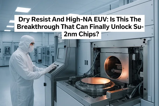
The semiconductor industry has entered one of its most critical phases. As the world moves into the AI era, the demand for denser, faster, and more energy-efficient chips has reached a breaking point. Traditional photolithography and wet resist processes are hitting physical limits, especially as manufacturers attempt to scale below the 2nm threshold. Two technologies are emerging as potential lifelines for sub-2nm production: dry resist deposition and high-numerical aperture extreme ultraviolet lithography, known as high-NA EUV. Together, they could hold the key to achieving the next leaps in performance at the 1.4nm and 1.0nm nodes. The recent collaboration between Lam Research Corporation (NASDAQ: LRCX) and JSR Corporation, parent of Inpria Corporation, has thrown fresh momentum into this race.
Why are dry resist processes gaining importance in the sub-2nm race?
Dry resist refers to resist materials and patterning processes that eliminate or drastically reduce the use of liquid chemicals in deposition and development. Instead of relying on spin coating or wet chemistry, dry resist uses plasma, atomic layer deposition, or other gas-phase methods to achieve extremely uniform thin films. This approach addresses one of the central issues in sub-2nm scaling: the limitations of chemically amplified resists.
Traditional resists face severe challenges as dimensions shrink. The chemical diffusion and variability inherent to wet processes create line-edge roughness and stochastic defects that become proportionally larger at smaller nodes. Dry resist technology offers a way to control uniformity at the atomic level, reduce variability, and improve pattern fidelity. Lam Research has invested heavily in this space, developing its Aether® dry resist platform. Tests conducted at imec demonstrated the ability of dry resist processes to achieve 28nm pitch patterns, providing confidence that such methods can be extended to high-NA EUV scanners.
Another benefit of dry resist is sustainability. Wet processes require large volumes of solvents and developer chemicals, while dry resist systems can reduce waste, energy consumption, and environmental risk. This sustainability advantage is increasingly relevant as fabs seek greener solutions without sacrificing yield.
Why are metal oxide resists considered critical for extending EUV lithography to sub-2nm nodes?
Metal oxide resists, pioneered by companies like Inpria, represent another key breakthrough. These materials, built on tin-oxide and similar chemistries, absorb EUV photons more effectively than conventional resists. They offer higher contrast and resolution under EUV exposure, enabling thinner resist films with sufficient etch resistance. Thinner films are crucial in high-NA EUV because they reduce depth-of-focus problems, but they must still deliver strong pattern transfer.
Inpria’s metal oxide resists have already been tested across leading foundries and research institutes, proving their ability to support advanced logic scaling. Yet challenges remain. These resists often require higher doses to achieve target performance, which can reduce throughput and increase costs. By integrating with Lam’s dry resist processes, the industry hopes to balance the benefits of higher absorption with reduced dose penalties, enabling practical sub-2nm production.
Why is high-NA EUV seen as the key technology for pushing semiconductor scaling below 2nm?
Extreme ultraviolet lithography has been the workhorse of leading-edge chips since the 7nm and 5nm nodes. But the 0.33 NA EUV tools currently in use face limitations in resolving smaller pitches without resorting to multiple patterning steps, which add complexity and cost. High-NA EUV, with a numerical aperture of around 0.55, dramatically improves resolution. It allows chipmakers to print smaller features in a single exposure, reducing the reliance on costly multi-patterning schemes.
However, high-NA EUV also creates new headaches. The depth of focus shrinks dramatically, requiring thinner resists and extremely precise wafer flatness. Overlay errors, mask defects, and line-edge roughness become even more damaging. Moreover, the first generation of high-NA scanners costs hundreds of millions of dollars each, limiting adoption to the largest players like Intel, TSMC, and Samsung.
This is where dry resist and metal oxide resists intersect with high-NA EUV. By providing higher sensitivity, thinner films, and improved etch compatibility, they can help overcome the practical hurdles of high-NA patterning. Together, they promise to bring high-NA EUV from the lab into volume manufacturing, potentially unlocking nodes below 2nm.
How do Lam Research and JSR Corporation position themselves in this landscape?
Lam Research’s dry resist technology and JSR’s Inpria division are combining forces through a cross-licensing and collaboration agreement announced in September 2025. The deal dismisses ongoing litigation and opens the door to co-develop advanced materials, precursors for atomic layer deposition, and new etch processes aligned with high-NA EUV requirements.
For Lam Research, this partnership strengthens its competitive moat in etch and deposition tools by integrating more tightly with resist materials. For JSR, it accelerates commercialization of Inpria’s metal oxide resists and expands their adoption into fabs deploying high-NA EUV systems. Both companies recognize that no single innovation will be enough; success depends on co-optimizing materials and tools at every stage of the process flow.
Industry watchers see the move as a signal that resist innovation is now as strategically important as lithography optics. It also shows how partnerships can reduce risks and accelerate roadmaps in a sector where time to market is everything.
What challenges still block the path to 1.4nm and 1.0nm production?
Even with these breakthroughs, several daunting obstacles stand in the way of sub-2nm commercialization.
Resist sensitivity remains a critical concern. Metal oxide resists may deliver high resolution but often at the cost of higher dose requirements, slowing throughput and raising tool operating costs. Defectivity is another unresolved issue, as stochastic failures—missing contacts, bridging lines, or pattern collapse—are increasingly likely at such small dimensions.
High-NA EUV itself is not a magic bullet. Its reduced depth of focus, coupled with thinner resist films, makes process integration highly sensitive. Overlay accuracy between layers must be nearly perfect, and any mask imperfections become magnified. On top of this, the economics of high-NA adoption are uncertain. With each scanner costing more than $350 million and requiring extensive fab modifications, only a handful of companies can afford the investment.
Lastly, supply chain constraints add risk. Precursor materials for dry resist and metal oxide resists often rely on specialized chemistries that could be impacted by geopolitical restrictions. Export controls and trade tensions add another layer of uncertainty to commercialization timelines.
Could dry resist and high-NA EUV really unlock the sub-2nm era?
The signs are cautiously optimistic. Research at imec and early demonstrations from Lam show that dry resist can deliver tighter patterns with reduced variability. Inpria’s metal oxide resists continue to attract interest as fabs evaluate their ability to extend EUV lithography to new pitches. High-NA EUV systems are being delivered and installed, with Intel and ASML already showcasing pilot runs.
If these elements come together, the first 1.4nm logic nodes could be feasible later this decade, with early 1.0nm demonstrations potentially following. But the journey from lab to fab is fraught with technical and economic risks. For investors, this means companies like Lam Research and JSR Corporation represent long-term bets on advanced lithography ecosystems rather than immediate revenue booms.
How could breakthroughs in dry resist and high-NA EUV reshape the global semiconductor ecosystem?
The push toward sub-2nm is not just about transistor scaling; it is about reshaping the entire semiconductor supply chain. Foundries that succeed in deploying dry resist and high-NA EUV will set the performance benchmarks for AI, cloud, and advanced computing. Toolmakers and materials suppliers who establish themselves early could gain durable market share.
This also has geopolitical consequences. Japan’s dominance in photoresists and materials, combined with U.S. leadership in tools, creates interdependencies that export controls and trade policies could disrupt. As nations invest in semiconductor sovereignty, breakthroughs like dry resist deposition and metal oxide resists may be treated as strategic assets.
Why dry resist and high-NA EUV mark a technology inflection point that could reshape chip manufacturing
Dry resist and high-NA EUV together represent one of the most promising pathways to sub-2nm logic nodes. They address fundamental physical limits while offering a roadmap for continued scaling. Yet, the risks are high, costs enormous, and timelines uncertain. The Lam Research–JSR partnership underscores the need for collaboration between equipment and material suppliers to align innovations and accelerate readiness.
If successful, this collaboration could redefine how chips are manufactured, pushing the industry past one of its toughest roadblocks. For fabs, suppliers, and investors, the outcome of this race will determine not just who leads at the 1.4nm and 1.0nm nodes, but who controls the foundation of the AI era.
Discover more from Business-News-Today.com
Subscribe to get the latest posts sent to your email.