


Siemens AG has acquired Canopus AI, a France-based specialist in AI-powered computational metrology, as part of its long-term strategy to strengthen its role in semiconductor manufacturing. The transaction, which closed on January 12, 2026, brings Canopus AI’s machine learning and inspection software into Siemens’ electronic design automation portfolio. This move further extends Siemens’ Calibre platform into angstrom-era wafer simulation and inspection, enabling chipmakers to accelerate yield ramp, improve process control, and gain predictive insight from increasingly complex manufacturing environments.
The acquisition positions Siemens to deliver a more integrated design-to-silicon feedback loop. By combining physical design verification with deep learning-based inspection and edge placement error analytics, the company is targeting a fundamental bottleneck in modern chip manufacturing: high-fidelity, high-throughput metrology for sub-3nm and post-EUV nodes.
Why Siemens is targeting AI-powered metrology as its next frontier in digital semiconductor twins
The acquisition signals Siemens’ deeper commitment to embedding industrial artificial intelligence into the most precision-demanding layers of semiconductor production. Metrology, which refers to the precise measurement of wafer and mask features during manufacturing, is no longer just a downstream quality-control step. In the angstrom era, it is central to predictive yield modeling, OPC calibration, and photomask verification.
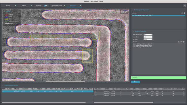
Canopus AI’s platform fills an emerging gap in this space. The company has developed a scalable, software-based metrology system that analyzes CD-SEM and TEM image data using proprietary neural networks. These models identify edge placement errors and pattern variability at scale, enabling fab engineers to detect and correct process drifts long before yield loss becomes visible. With the ability to automatically process hundreds of thousands of SEM images, the platform can surface key deviations, flag contour shifts, and even simulate missing layers via synthetic image generation.
By integrating Canopus AI’s capabilities into the Calibre platform, Siemens is building a tighter simulation loop that bridges design and manufacturing with shared data. The result is a more complete semiconductor digital twin architecture, one that continuously learns from actual wafer data and feeds those learnings back into model refinement, mask optimization, and pattern fidelity improvement.
How Canopus AI enhances Siemens’ Calibre platform for yield modeling and process control
The Calibre platform is already used extensively for layout verification, rule checking, OPC, and manufacturing simulation. What Canopus AI adds is a metrology-driven inspection layer that complements and expands Calibre’s runtime intelligence. Together, the combined system can now perform real-time contour extraction, pattern recognition, and process window characterization based on actual SEM imagery.
This creates a powerful workflow enhancement. Foundries and integrated device manufacturers using Siemens’ EDA tools can now ingest inline manufacturing data to tune OPC models with higher accuracy. Edge placement error-based calibration becomes feasible not just during initial tape-out, but throughout the yield ramp phase. Process control parameters, like focus-exposure conditions or dose variation, can be automatically modeled using AI-derived process windows generated from metrology data.
These capabilities are not theoretical. Canopus AI’s SEM EPE measurement engine has already demonstrated ability to handle advanced multigon geometries and support pixel-to-vertex-based data formats, including curvilinear features. It integrates seamlessly with Siemens’ OPC and contour-based modeling tools, allowing for tighter OPC-etch model calibration and sub-nanometer mask tuning.
In short, Canopus AI unlocks an entirely new layer of fidelity for Calibre’s users, enabling fabs to act on metrology data with model-backed insight instead of relying on reactive correction after yield issues have materialized.
What the Canopus AI acquisition reveals about Siemens’ industrial AI ambitions in chip design
Siemens has consistently positioned itself as a leader in digitalization across multiple industrial verticals, but the Canopus AI acquisition signals a sharp focus on verticalized AI for semiconductor precision engineering. Rather than offering a generic AI toolkit, Siemens is now embedding algorithmic intelligence into the most metrology-intensive workflows in chipmaking.
This marks a broader strategic evolution for Siemens. The company is clearly investing in domain-specific artificial intelligence that works natively with wafer-scale imagery, process control data, and lithographic simulation environments. The metrology vertical is particularly suited for such investment because it suffers from high manual analysis burden, limited interoperability across equipment vendors, and an urgent need to accelerate throughput without sacrificing resolution.
With Canopus AI now integrated, Siemens gains a native AI capability built from the ground up for inspection and manufacturing variability analysis. The acquired company’s “Metrospection” concept—a term coined to describe the fusion of inspection and metrology using artificial intelligence—creates a holistic view of wafer health that is uniquely valuable in sub-5nm and memory-intensive applications.
This signals to both customers and competitors that Siemens is not content to remain a design-only player in EDA. Instead, it is positioning to own a continuous loop from design signoff to process-aware inspection, process model correction, and ultimately real-time yield optimization.
Why competitors in EDA and metrology will need to respond to Siemens’ strategic positioning
The acquisition will not go unnoticed by Siemens’ closest rivals. Synopsys Inc. and Cadence Design Systems Inc., the two other giants in the EDA landscape, have invested in AI for logic design, analog layout, and verification, but have yet to move decisively into inline metrology and defect inspection. KLA Corporation, meanwhile, dominates inspection hardware and data systems, but operates primarily in the physical tooling layer.
With Canopus AI, Siemens becomes the first among its peers to directly merge OPC-aware lithography modeling with AI-powered metrology and SEM-based contour analytics. This capability gives Siemens a unique ability to offer a unified feedback architecture across the design-to-yield continuum.
This may compel rivals to look for acquisitions of their own, particularly in areas like AI-based inspection, synthetic SEM image generation, and massive EPE-based gauge systems. For foundries and logic chipmakers, the ability to unify process-aware simulation with post-silicon image analytics is increasingly vital to achieve cost-effective yield ramping, especially when photomasks can cost tens of millions of dollars per layer.
Canopus AI’s toolset, now under Siemens’ umbrella, could also reduce dependency on fab-specific metrology workflows, allowing design engineers to simulate downstream effects with higher confidence during earlier stages of PDK development and device tape-out.
What execution risks Siemens must manage as it integrates Canopus AI into its software stack
While the strategic logic is sound, the execution of this integration will require careful orchestration. First, Siemens must ensure compatibility with a broad array of SEM tools from vendors like Applied Materials, Hitachi High-Tech, and Thermo Fisher Scientific. Canopus AI’s software is hardware-agnostic, but EDA-fab interoperability is notoriously tricky, and runtime alignment across fabs may require new interface layers or plugins.
Second, data harmonization will be a challenge. SEM image formats, magnification scaling, and EPE gauge standards are not universally aligned across fabs. Siemens will need to ensure its model calibration engines are robust to these variances without producing false-positive defect signatures or under-predicting process drift.
Third, the pace of feature rollout must be preserved. Canopus AI has historically been agile and responsive, shipping rapid updates for evolving OPC and EUV patterning requirements. Large acquirers often unintentionally dampen this velocity. Siemens will need to protect and amplify the innovation tempo while integrating roadmap priorities into the broader Calibre suite.
Finally, commercial go-to-market decisions such as packaging, licensing, and support will impact customer perception. Siemens must avoid creating artificial segmentation between Calibre and Canopus AI’s capabilities that could confuse customers or dilute ROI narratives.
How Siemens may reshape the future of EDA and metrology through this acquisition
The long-term implications of this deal suggest Siemens is preparing to operate at a higher plane of the semiconductor value chain. Rather than functioning as a signoff tool supplier, it may evolve into an end-to-end simulation platform for manufacturing performance.
With Canopus AI, Siemens now has the building blocks for a full-stack offering that includes design-aware inspection, process model tuning, mask correction, and in-fab feedback loops—all enhanced by artificial intelligence. This could eventually expand into services such as real-time defect prevention, pattern migration modeling, and next-gen mask synthesis optimization.
As the semiconductor industry moves toward design–manufacturing co-optimization at the angstrom scale, the firms that can close the loop between silicon design and silicon behavior will define the next generation of yield leaders. Siemens, through this acquisition, is making a strong bid to be one of them.
What Siemens’ acquisition of Canopus AI means for advanced chip manufacturing and inspection
Siemens AG has expanded its semiconductor software stack by acquiring Canopus AI, a specialist in AI-powered metrology for advanced wafer and mask inspection. The deal strengthens Siemens’ Calibre platform and positions the company to offer more predictive, yield-centric design-to-manufacturing workflows.
By integrating Canopus AI’s edge placement error analytics, synthetic SEM and TEM generation, and curvilinear mask support into Calibre, Siemens is building a unified platform that addresses core challenges in sub-3nm and angstrom-era semiconductor production.
This move raises the bar for competitors in both EDA and physical inspection and signals Siemens’ intent to become a full-stack provider in AI-augmented semiconductor workflows. It also highlights a broader trend toward industrial AI adoption in metrology-heavy domains.
Siemens must still manage key risks around integration, tool compatibility, and roadmap cohesion. But if executed well, the acquisition gives Siemens a powerful strategic edge in delivering digital twins that are not just design-aware, but yield-driven and process-calibrated.
Key takeaways: What Siemens’ acquisition of Canopus AI means for semiconductor manufacturing
- Siemens AG has acquired Canopus AI to enhance its Calibre platform with AI-powered metrology and inspection capabilities.
- The acquisition targets sub-nanometer process control challenges in advanced semiconductor manufacturing.
- Canopus AI brings SEM EPE metrology, synthetic SEM/TEM generation, and curvilinear data processing into Siemens’ EDA ecosystem.
- The deal expands Siemens’ digital thread from OPC verification to real-time yield feedback and process tuning.
- Siemens now competes more directly with metrology and inspection incumbents, potentially shifting value away from hardware-tied workflows.
- Competitors like Synopsys and Cadence may feel pressure to match Siemens’ vertical AI integration in design-to-manufacturing.
- Integration risks include tool interoperability, scaling data formats, and ensuring seamless adoption across fab environments.
- The acquisition underscores Siemens’ broader strategy of embedding domain-specific AI across high-precision manufacturing verticals.
- Long-term, Siemens could evolve into a unified simulation, metrology, and digital twin platform for semiconductor fabs.
- This move reinforces the growing role of AI in addressing manufacturing variability and accelerating yield in the angstrom era.
Discover more from Business-News-Today.com
Subscribe to get the latest posts sent to your email.