


HyperLight Corporation has introduced a 145 GHz packaged intensity modulator and simultaneously expanded its manufacturing partnerships with United Microelectronics Corporation and Jabil Inc. to accelerate deployment of thin-film lithium niobate photonics in hyperscale artificial intelligence infrastructure. The announcements position HyperLight Corporation’s TFLN chiplet platform as a potential foundation for next-generation optical interconnects capable of supporting 448Gbps per lane data transmission and 260GBaud coherent telecom links. By combining device innovation with high-volume semiconductor foundry manufacturing and system integration capacity, the collaboration seeks to move advanced photonics from laboratory-scale deployment into mainstream data-center infrastructure. The strategic significance lies in addressing the emerging bandwidth and power challenges created by increasingly dense artificial intelligence clusters.
Why are AI data centers increasingly constrained by optical interconnect bandwidth and power efficiency limits?
The rapid expansion of generative artificial intelligence workloads is pushing hyperscale data centers toward a structural networking bottleneck. Graphics processing units and AI accelerators can scale compute density rapidly, but the optical links connecting these processors often struggle to keep pace with bandwidth requirements. Optical interconnect technology therefore becomes the invisible infrastructure that determines whether new AI clusters can actually deliver the computational throughput their hardware promises.
Current optical transceiver architectures rely heavily on conventional silicon photonics and externally modulated lasers. While these systems have improved significantly over the past decade, their power consumption and signal fidelity begin to strain under extremely high symbol rates. As link speeds move toward 800G, 1.6T, and beyond, the optical layer risks becoming the dominant energy consumer in data-center networking.
Thin-film lithium niobate photonics has emerged as a possible solution because the material enables extremely high electro-optic bandwidth while maintaining relatively low drive voltages. In simple terms, the technology can transmit more data per optical channel while requiring less electrical energy to do so. For hyperscale operators running clusters with tens of thousands of GPUs, even small efficiency improvements per optical module can translate into measurable reductions in facility-level energy demand.
HyperLight Corporation’s push to commercialize TFLN devices therefore targets a specific industry problem. The company is attempting to eliminate one of the structural friction points in AI infrastructure scaling.
How does HyperLight’s 145 GHz intensity modulator address the next generation of 448Gbps optical networking lanes?
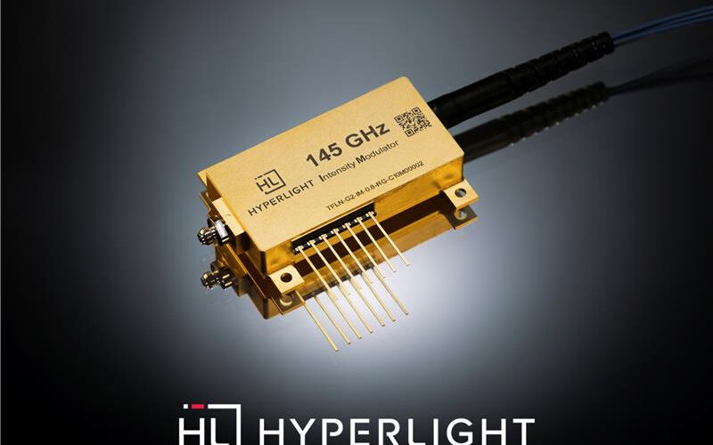
The newly introduced packaged intensity modulator is designed to operate with electro-optical bandwidth exceeding 145 GHz. This specification places the device among the fastest packaged modulators currently available for commercial optical system development.
High-bandwidth modulators are essential because they directly determine how quickly information can be encoded onto optical signals. If the modulator cannot operate at extremely high frequencies, the overall transmission speed of the optical link is limited regardless of how advanced the rest of the network hardware may be.
The device released by HyperLight Corporation is engineered to support 448Gbps per lane intensity-modulated direct-detection links, which are expected to become a building block for future high-capacity data-center interconnects. It is also capable of supporting 260GBaud coherent communication systems that dominate long-distance telecom and metro network infrastructure.
From a system engineering perspective, the modulator’s design addresses multiple practical constraints simultaneously. The component integrates polarization-maintaining optical fiber, supports multiple wavelength bands including O-band, C-band, L-band and 1µm configurations, and includes a high-frequency RF connector interface designed for laboratory testing and system prototyping environments.
These engineering choices suggest that HyperLight Corporation is not only targeting future production optical modules but also attempting to establish its technology as a development standard within advanced photonics laboratories and optical system design teams.
Why does scaling thin-film lithium niobate manufacturing matter for the commercialization of photonic technologies?
Innovations in photonic materials often stall not because of performance limitations but because manufacturing scale remains difficult to achieve. Thin-film lithium niobate has long been recognized as a promising electro-optic material, yet historically it has remained confined to specialized research environments or limited production runs.
The strategic partnership between HyperLight Corporation, United Microelectronics Corporation, and Wavetek Microelectronics Corporation attempts to solve that commercialization barrier. By integrating TFLN devices into established semiconductor foundry manufacturing lines capable of processing 6-inch and 8-inch wafers, the partnership creates a pathway toward large-scale production capacity.
United Microelectronics Corporation brings decades of semiconductor fabrication expertise and global manufacturing infrastructure to the effort. Wavetek Microelectronics Corporation contributes experience translating laboratory photonics technology into qualified foundry processes. HyperLight Corporation itself acts as the architectural designer of the TFLN chiplet platform that integrates these devices into optical module systems.
This manufacturing structure resembles the ecosystem model used by the semiconductor industry. A technology developer defines the architecture while established foundries provide scalable production capacity. The approach reduces capital requirements for the technology innovator while allowing the platform to reach global markets more quickly.
How does the Jabil manufacturing collaboration move TFLN photonics from component innovation to system-level deployment?
Scaling device manufacturing alone does not guarantee commercial adoption. Optical technologies must also integrate smoothly into the complex supply chains that produce data-center hardware. The collaboration with Jabil Inc. addresses that system-integration challenge. Jabil Inc. specializes in high-volume electronics manufacturing and supply-chain coordination, making it a natural partner for turning photonic components into production-ready optical modules.
In hyperscale infrastructure environments, system reliability and manufacturability matter as much as raw performance. Data-center operators typically prefer components that can be deployed in massive quantities with predictable supply chains and consistent quality control. Jabil Inc.’s involvement therefore suggests that the TFLN platform is transitioning from experimental photonics technology toward an industrial manufacturing model capable of serving hyperscale customers.
For artificial intelligence infrastructure, the timing is significant. AI clusters are expanding so rapidly that the networking layer must evolve in parallel with compute hardware. Optical interconnect vendors that can deliver both performance and supply-chain reliability will likely capture the largest share of this expanding market.
Could thin-film lithium niobate photonics become the foundation for 1.6T and future optical networking standards?
Optical networking roadmaps already anticipate transmission speeds exceeding 1.6 terabits per second per module. Achieving such performance levels will require both higher symbol rates and more efficient optical modulation architectures.
Thin-film lithium niobate technology may provide one of the few practical paths toward those targets. The material supports extremely high modulation bandwidth and can operate with lower drive voltages than many conventional photonic approaches.
Lower drive voltage matters because it allows photonic devices to interface more efficiently with complementary metal oxide semiconductor electronics. As optical engines become increasingly integrated with switch chips and network processors, compatibility with standard semiconductor voltage levels becomes a critical design advantage.
Another potential benefit involves laser count. Certain TFLN architectures can reduce the number of lasers required within optical modules, lowering both cost and power consumption. At hyperscale deployment levels, these incremental improvements compound across thousands of networking links.
In effect, the technology promises both performance gains and operational efficiency improvements, which explains why hyperscale operators are monitoring the development of TFLN platforms closely.
What execution risks and competitive pressures could shape HyperLight’s future in the photonics infrastructure market?
Despite the technical promise of thin-film lithium niobate, several execution risks remain. Manufacturing photonic devices at semiconductor-scale volumes requires extremely tight process control. Any yield variability or reliability concerns could slow adoption among hyperscale operators that demand strict component validation standards.
Competitive dynamics also remain intense. Silicon photonics continues to evolve rapidly, supported by major semiconductor companies and large optical networking vendors. Those incumbents benefit from established manufacturing ecosystems and existing relationships with hyperscale customers.
HyperLight Corporation must therefore prove that TFLN photonics offers not only theoretical advantages but also measurable cost, performance, and reliability benefits in real-world deployments.
Another factor involves ecosystem maturity. Optical networking standards evolve through collaboration among multiple hardware vendors, component suppliers, and hyperscale operators. For TFLN technology to become a dominant platform, a broader ecosystem of compatible components and system architectures will need to emerge. Nonetheless, the combination of device innovation, semiconductor foundry partnerships, and high-volume manufacturing integration suggests that HyperLight Corporation is positioning itself strategically within this emerging photonics landscape.
What does HyperLight’s recent announcements signal about the future direction of optical networking infrastructure?
Taken together, HyperLight Corporation’s announcements highlight an industry shift toward integrating photonics development more closely with semiconductor manufacturing ecosystems. The strategy mirrors the evolution of advanced chip technologies, where scale and supply-chain coordination often determine commercial success.
As artificial intelligence workloads continue expanding, the networking infrastructure connecting these systems will become increasingly critical. Optical interconnect technologies capable of delivering higher bandwidth while controlling energy consumption are likely to attract significant investment and industry attention.
HyperLight Corporation’s approach combines three key ingredients necessary for commercialization. First, it introduces high-performance photonic devices capable of meeting next-generation bandwidth requirements. Second, it secures semiconductor-grade manufacturing capacity through partnerships with established foundries. Third, it integrates system-level manufacturing expertise through collaboration with Jabil Inc.
Whether the TFLN platform ultimately becomes a dominant technology remains uncertain, but the company’s recent moves clearly indicate that the race to redefine optical networking infrastructure for the AI era is intensifying.
Key takeaways on what HyperLight’s TFLN photonics strategy means for AI networking infrastructure
- HyperLight Corporation is attempting to commercialize thin-film lithium niobate photonics as a scalable platform for high-speed optical networking.
- The company’s new 145 GHz packaged intensity modulator targets next-generation 448Gbps per lane data-center interconnect architectures.
- Partnerships with United Microelectronics Corporation and Wavetek Microelectronics Corporation establish a semiconductor-scale manufacturing pathway for TFLN devices.
- Collaboration with Jabil Inc. introduces high-volume system integration capabilities necessary for hyperscale deployment.
- Thin-film lithium niobate photonics offers potential advantages in bandwidth, drive voltage efficiency, and laser count reduction compared with some incumbent technologies.
- AI infrastructure growth is intensifying demand for optical interconnects that can scale beyond current silicon photonics limits.
- Manufacturing scalability and ecosystem adoption remain key execution challenges for emerging photonic platforms.
- If successfully commercialized, TFLN photonics could influence the design of 800G, 1.6T, and future optical networking standards.
- The announcements signal that advanced photonics technologies are moving closer to mainstream semiconductor manufacturing environments.
- For hyperscale data-center operators, improvements in optical efficiency could translate directly into greater compute density and lower infrastructure energy consumption.
Discover more from Business-News-Today.com
Subscribe to get the latest posts sent to your email.